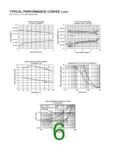
OFFSET TRIMMING
The INA128/INA129 is laser trimmed for low offset voltage
and offset voltage drift. Most applications require no exter-
nal offset adjustment. Figure 2 shows an optional circuit for
trimming the output offset voltage. The voltage applied to
Ref terminal is summed with the output. The op amp buffer
provides low impedance at the Ref terminal to preserve good
common-mode rejection.
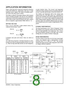
Microphone,
Hydrophone
etc.
INA128
47kΩ
47kΩ
–
VIN
Thermocouple
INA128
V+
VO
RG
INA128
Ref
100µA
1/2 REF200
+
VIN
10kΩ
100Ω
100Ω
10kΩ
OPA177
±10mV
Adjustment Range
INA128
100µA
1/2 REF200
Center-tap provides
bias current return.
V–
FIGURE 2. Optional Trimming of Output Offset Voltage.
FIGURE 3. Providing an Input Common-Mode Current Path.
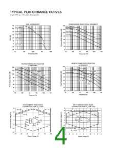
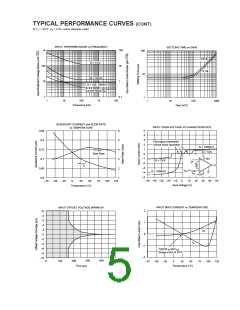
INPUT BIAS CURRENT RETURN PATH
linear common-mode input range is related to the output
voltage of the complete amplifier. This behavior also de-
pends on supply voltage—see performance curves “Input
Common-Mode Range vs Output Voltage”.
The input impedance of the INA128/INA129 is extremely
high—approximately 1010Ω. However, a path must be pro-
vided for the input bias current of both inputs. This input
bias current is approximately ±2nA. High input impedance
means that this input bias current changes very little with
varying input voltage.
Input-overload can produce an output voltage that appears
normal. For example, if an input overload condition drives
both input amplifiers to their positive output swing limit, the
difference voltage measured by the output amplifier will be
near zero. The output of A3 will be near 0V even though both
inputs are overloaded.
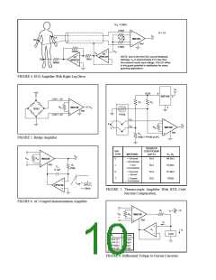
Input circuitry must provide a path for this input bias current
for proper operation. Figure 3 shows various provisions for
an input bias current path. Without a bias current path, the
inputs will float to a potential which exceeds the common-
mode range, and the input amplifiers will saturate.
LOW VOLTAGE OPERATION
If the differential source resistance is low, the bias current
return path can be connected to one input (see the thermo-
couple example in Figure 3). With higher source impedance,
using two equal resistors provides a balanced input with
possible advantages of lower input offset voltage due to bias
current and better high-frequency common-mode rejection.
The INA128/INA129 can be operated on power supplies as
low as ±2.25V. Performance remains excellent with power
supplies ranging from ±2.25V to ±18V. Most parameters
vary only slightly throughout this supply voltage range—see
typical performance curves. Operation at very low supply
voltage requires careful attention to assure that the input
voltages remain within their linear range. Voltage swing
requirements of internal nodes limit the input common-
mode range with low power supply voltage. Typical perfor-
mance curves, “Input Common-Mode Range vs Output
Voltage” show the range of linear operation for ±15V, ±5V,
and ±2.5V supplies.
INPUT COMMON-MODE RANGE
The linear input voltage range of the input circuitry of the
INA128/INA129 is from approximately 1.4V below the
positive supply voltage to 1.7V above the negative supply.
As a differential input voltage causes the output voltage
increase, however, the linear input range will be limited by
the output voltage swing of amplifiers A1 and A2. So the

 BB [ BURR-BROWN CORPORATION ]