range for a 0V to +VDD analog input. This external reference
can be as low as 50mV.
THEORY OF OPERATION
The ADS7830 is a classic Successive Approximation Regis-
ter (SAR) A/D converter. The architecture is based on ca-
pacitive redistribution which inherently includes a sample-
and-hold function. The converter is fabricated on a 0.6µ
CMOS process.
As the reference voltage is reduced, the analog voltage
weight of each digital output code is reduced. This is often
referred to as the LSB (least significant bit) size and is equal
to the reference voltage divided by 256. This means that any
offset or gain error inherent in the A/D converter will appear
to increase, in terms of LSB size, as the reference voltage is
reduced.
The ADS7830 core is controlled by an internally generated
free-running clock. When the ADS7830 is not performing
conversions or being addressed, it keeps the A/D converter
core powered off, and the internal clock does not operate.
The noise inherent in the converter will also appear to increase
with lower LSB size. With a 2.5V reference, the internal noise
of the converter typically contributes only 0.02LSB peak-to-
peak of potential error to the output code. When the external
reference is 50mV, the potential error contribution from the
internal noise will be 50 times larger—1LSB. The errors due to
the internal noise are Gaussian in nature and can be reduced
by averaging consecutive conversion results.
The simplified diagram of input and output for the ADS7830
is shown in Figure 1.
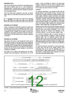
ANALOG INPUT
When the converter enters the hold mode, the voltage on the
selected CHx pin is captured on the internal capacitor array.
The input current on the analog inputs depends on the
conversion rate of the device. During the sample period, the
source must charge the internal sampling capacitor (typically
25pF). After the capacitor has been fully charged, there is no
further input current. The amount of charge transfer from the
analog source to the converter is a function of conversion rate.
DIGITAL INTERFACE
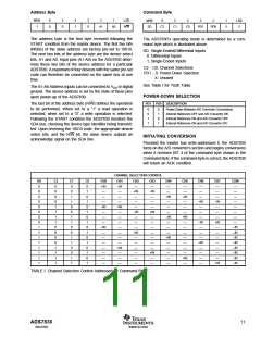
The ADS7830 supports the I2C serial bus and data transmis-
sion protocol, in all three defined modes: standard, fast, and
high-speed. A device that sends data onto the bus is defined
as a transmitter, and a device receiving data as a receiver.
The device that controls the message is called a “master.”
The devices that are controlled by the master are “slaves.”
The bus must be controlled by a master device that gener-
ates the serial clock (SCL), controls the bus access, and
generates the START and STOP conditions. The ADS7830
operates as a slave on the I2C bus. Connections to the bus
are made via the open-drain I/O lines SDA and SCL.
REFERENCE
The ADS7830 can operate with its internal 2.5V reference or
an external reference. When using a +2.7V supply, the
internal 2.5V reference will provide full dynamic range for a
0V to +VDD analog input. If a +5V supply is used, an external
5V reference is required in order to provide full dynamic
+2.7V to +3.6V
5Ω
+
1µF to
10µF
2kΩ
2kΩ
REFIN
/
VDD
+
REFOUT
0.1µF
1µF to
10µF
Microcontroller
CH0
SDA
CH1
CH2
SCL
A0
ADS7828
CH3
CH4
CH5
CH6
CH7
COM
A1
GND
FIGURE 1. Simplified I/O of the ADS7830.
ADS7830
9
www.ti.com
SBAS302

 BB [ BURR-BROWN CORPORATION ]