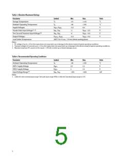
Table 5. Absolute Maximum Ratings
Parameter
Symbol
Min.
–ꢁꢁ
–40
–0.ꢁ
–2
Max.
Units
°C
°C
V
Storage Temperature
Ambient Operating Temperature
Supply Voltages
Steady-State Input Voltage [±, ꢀ]
Two-Second Transient Input Voltage [2]
Output Voltages
TS
+±2ꢁ
TA
+±0ꢁ
VDD±, VDD2
VIN+, VIN–
VIN+, VIN–
VOUT+, VOUT–
6.0
VDD± + 0.ꢁ
VDD± + 0.ꢁ
VDD2 + 0.ꢁ
V
–6
V
–0.ꢁ
V
Lead Solder Temperature
Notes:
260°C for ±0 sec., ±.6 mm below seating plane
±. DC voltage of up to –2 V on the inputs does not cause latch-up or damage to the device; tested at typical operating conditions.
2. Transient voltage of 2 seconds up to –6 V on the inputs does not cause latch-up or damage to the device; tested at typical operating conditions.
ꢀ. Absolute maximum DC current on the inputs = ±00 mA, no latch-up or device damage occurs.
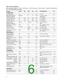
Table 6. Recommended Operating Conditions
Parameter
Symbol
TA
Min.
–40
4.ꢁ
Max.
+±0ꢁ
ꢁ.ꢁ
Units
°C
Ambient Operating Temperature
VDD± Supply Voltage
VDD2 Supply Voltage
Input Voltage Range [±]
Notes:
VDD±
V
VDD2
ꢀ
ꢁ.ꢁ
V
VIN+, VIN–
–200
+200
mV
±. ±200 mV is the nominal input range. Full scale input range (FSR) is ±ꢀ00 mV. Functional input range is ±2 V.
ꢁ

 AVAGO [ AVAGO TECHNOLOGIES LIMITED ]