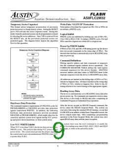
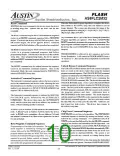
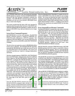
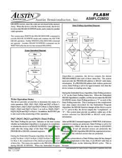
AUSTIN SEMICONDUCTOR, INC.
FLASH
AS8FLC2M32
Austin Semiconductor, Inc.
Command Definition Table
Bus Cycles (Notes 2-4)
First
Second
Third
Fourth
Fifth
Sixth
Command Sequence
(Note 1)
Addr
Data
Addr
Data
Addr
Data
Addr
Data
Addr
Data
Addr
Data
Read (Note 5)
Reset (Note 6)
Manufacturer ID
1
1
4
RA
RD
F0
XXX
AAA
AA
555
55
AAA
90
X00
1
Auto-Select
(Note 7)
Device ID, Btm. Boot
Sector Protect Verify
(Note 8)
4
4
AAA
AAA
AA
AA
555
555
55
55
AAA
AAA
90
90
X01
(SA)
X04
PA
37
0
1
Program
4
3
2
AAA
AAA
XXX
AA
AA
A0
555
555
PA
55
55
AAA
AAA
A0
20
PD
Unlock Bypass
Unlock Bypass Program
(Note 9)
PD
Unlock Bypass Reset
(Note 10)
2
XXX
90
XXX
0
Chip Erase
6
6
1
1
AAA
AAA
XXX
XXX
AA
AA
B0
30
555
555
55
55
AAA
AAA
80
80
AAA
AAA
AA
AA
555
555
55
55
AAA
SA
10
30
Sector Erase
Erase Suspend (Note 11)
Erase Resume (Note 12)
Legend:
X= Don't Care
RA = Address of the memory location to be read
RD = Data read from location RA during read operation
PA = Address of the memory location to be programmed. Addresses latched on the falling edge of the Wex\ or Cex\ pulse, whichever occurs later.
PD = Data to be programmed at location PA. Data latches on the rising edge of WE# or CE# pulse, whichever occurs later.
SA = Address of the sector to be verified (in autoselect mode) or erased. Address bits A20-A13 uniquely select any sector.
Notes:
1.See Table 1 for Valid Bus Operations.
2.All values in hexadecimal.
3.Except when reading array or autoselect data, all bus cycles are write operations
4.Data bits A20-A11 are don’t cares for unlock and command cycles
5.No unlock or command cycles required when reading array data.
6.The Reset command is required to return to reading array data when device is in the autoselect mode, or if DQ% goes high (while the device is providing status data).
7.The fourth cycle of the autoselect command sequence is a read cycle
8.The data is 00h for an unprotected sector and 01h for a protected sector.
9.The Unlock Bypass command is required prior to the Unlock Bypass Program command.
10.The Unlock Bypass Reset command is required to return to reading array data when the device is in the unlock bypass mode.
11. The system may read and program in non-erasing sectors, or enter the autoselect mode, when in the Erase Suspend mode.
The Erase Suspend command is valid only during a sector erase operation.
12. The Erase Resume command is valid only during the Erase Suspend mode.
*Data is for single byte.
BYTE 1 = DQ0 - DQ7
BYTE 2 = DQ8 - DQ15
BYTE 3 = DQ16 - DQ23
BYTE 4 = DQ24 - DQ31
Austin Semiconductor, Inc. reserves the right to change products or specifications without notice.
AS8FLC2M32B
Rev. 1.2 5/09
13

 AUSTIN [ AUSTIN SEMICONDUCTOR ]