ATmega64A
cleared on the Compare Match between TCNTn and OCRnx while upcounting, and set on the
Compare Match while downcounting. In inverting Output Compare mode, the operation is
inverted. The dual-slope operation has lower maximum operation frequency than single slope
operation. However, due to the symmetric feature of the dual-slope PWM modes, these modes
are preferred for motor control applications.
The PWM resolution for the phase correct PWM mode can be fixed to 8-, 9-, or 10-bit, or defined
by either ICRn or OCRnA. The minimum resolution allowed is 2-bit (ICRn or OCRnA set to
0x0003), and the maximum resolution is 16-bit (ICRn or OCRnA set to MAX). The PWM resolu-
tion in bits can be calculated by using the following equation:
log(TOP + 1)
R
= ----------------------------------
PCPWM
log(2)
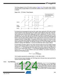
In phase correct PWM mode the counter is incremented until the counter value matches either
one of the fixed values 0x00FF, 0x01FF, or 0x03FF (WGMn3:0 = 1, 2, or 3), the value in ICRn
(WGMn3:0 = 10), or the value in OCRnA (WGMn3:0 = 11). The counter has then reached the
TOP and changes the count direction. The TCNTn value will be equal to TOP for one timer clock
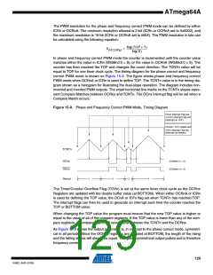
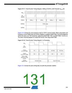
cycle. The timing diagram for the phase correct PWM mode is shown on Figure 15-8. The figure
shows phase correct PWM mode when OCRnA or ICRn is used to define TOP. The TCNTn
value is in the timing diagram shown as a histogram for illustrating the dual-slope operation. The
diagram includes non-inverted and inverted PWM outputs. The small horizontal line marks on
the TCNTn slopes represent Compare Matches between OCRnx and TCNTn. The OCnx inter-
rupt flag will be set when a Compare Match occurs.
Figure 15-8. Phase Correct PWM Mode, Timing Diagram
OCRnx / TOP Update and
OCnA Interrupt Flag Set
or ICFn Interrupt Flag Set
(Interrupt on TOP)
TOVn Interrupt Flag Set
(Interrupt on Bottom)
TCNTn
(COMnx1:0 = 2)
OCnx
(COMnx1:0 = 3)
OCnx
1
2
3
4
Period
The Timer/Counter Overflow Flag (TOVn) is set each time the counter reaches BOTTOM. When
either OCRnA or ICRn is used for defining the TOP value, the OCnA or ICFn flag is set accord-
ingly at the same timer clock cycle as the OCRnx Registers are updated with the double buffer
value (at TOP). The interrupt flags can be used to generate an interrupt each time the counter
reaches the TOP or BOTTOM value.
When changing the TOP value the program must ensure that the new TOP value is higher or
equal to the value of all of the compare registers. If the TOP value is lower than any of the com-
127
8160C–AVR–07/09

 ATMEL [ ATMEL ]