ATmega64A
that when using fixed TOP values the unused bits are masked to zero when any of the OCRnx
Registers are written.
The procedure for updating ICRn differs from updating OCRnA when used for defining the TOP
value. The ICRn Register is not double buffered. This means that if ICRn is changed to a low
value when the counter is running with none or a low prescaler value, there is a risk that the new
ICRn value written is lower than the current value of TCNTn. The result will then be that the
counter will miss the Compare Match at the TOP value. The counter will then have to count to
the MAX value (0xFFFF) and wrap around starting at 0x0000 before the Compare Match can
occur. The OCRnA Register however, is double buffered. This feature allows the OCRnA I/O
location to be written anytime. When the OCRnA I/O location is written the value written will be
put into the OCRnA Buffer Register. The OCRnA Compare Register will then be updated with
the value in the buffer register at the next timer clock cycle the TCNTn matches TOP. The
update is done at the same timer clock cycle as the TCNTn is cleared and the TOVn flag is set.
Using the ICRn Register for defining TOP works well when using fixed TOP values. By using
ICRn, the OCRnA Register is free to be used for generating a PWM output on OCnA. However,
if the base PWM frequency is actively changed (by changing the TOP value), using the OCRnA
as TOP is clearly a better choice due to its double buffer feature.
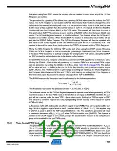
In fast PWM mode, the compare units allow generation of PWM waveforms on the OCnx pins.
Setting the COMnx1:0 bits to two will produce a non-inverted PWM and an inverted PWM output
can be generated by setting the COMnx1:0 to three (See Table 15-3 on page 134). The actual
OCnx value will only be visible on the port pin if the data direction for the port pin is set as output
(DDR_OCnx). The PWM waveform is generated by setting (or clearing) the OCnx Register at
the Compare Match between OCRnx and TCNTn, and clearing (or setting) the OCnx Register at
the timer clock cycle the counter is cleared (changes from TOP to BOTTOM).
The PWM frequency for the output can be calculated by the following equation:
f
clk_I/O
f
= ----------------------------------
OCnxPWM
N ⋅ (1 + TOP)
The N variable represents the prescaler divider (1, 8, 64, 256, or 1024).
The extreme values for the OCRnx Register represents special cases when generating a PWM
waveform output in the fast PWM mode. If the OCRnx is set equal to BOTTOM (0x0000) the out-
put will be a narrow spike for each TOP+1 timer clock cycle. Setting the OCRnx equal to TOP
will result in a constant high or low output (depending on the polarity of the output set by the
COMnx1:0 bits.)
A frequency (with 50% duty cycle) waveform output in fast PWM mode can be achieved by set-
ting OCnA to toggle its logical level on each Compare Match (COMnA1:0 = 1). This applies only
if OCRnA is used to define the TOP value (WGMn3:0 = 15). The waveform generated will have
a maximum frequency of fOC A = fclk_I/O/2 when OCRnA is set to zero (0x0000). This feature is
n
similar to the OCnA toggle in CTC mode, except the double buffer feature of the Output Com-
pare unit is enabled in the fast PWM mode.
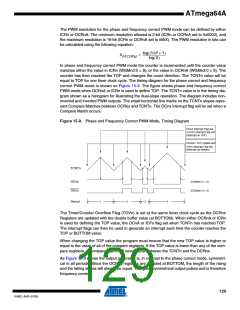
15.9.4
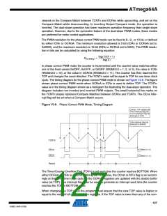
Phase Correct PWM Mode
The phase correct Pulse Width Modulation or phase correct PWM mode (WGMn3:0 = 1, 2, 3,
10, or 11) provides a high resolution phase correct PWM waveform generation option. The
phase correct PWM mode is, like the phase and frequency correct PWM mode, based on a dual-
slope operation. The counter counts repeatedly from BOTTOM (0x0000) to TOP and then from
TOP to BOTTOM. In non-inverting Compare Output mode, the Output Compare (OCnx) is
126
8160C–AVR–07/09

 ATMEL [ ATMEL ]