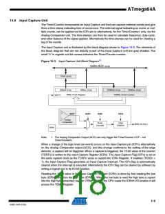
ATmega64A
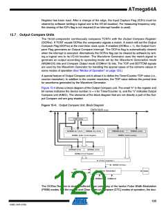
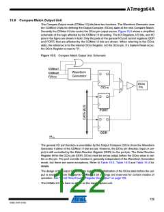
15.8 Compare Match Output Unit
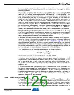
The Compare Output mode (COMnx1:0) bits have two functions. The Waveform Generator uses
the COMnx1:0 bits for defining the Output Compare (OCnx) state at the next Compare Match.
Secondly the COMnx1:0 bits control the OCnx pin output source. Figure 15-5 shows a simplified
schematic of the logic affected by the COMnx1:0 bit setting. The I/O Registers, I/O bits, and I/O
pins in the figure are shown in bold. Only the parts of the general I/O port control registers (DDR
and PORT) that are affected by the COMnx1:0 bits are shown. When referring to the OCnx
state, the reference is for the internal OCnx Register, not the OCnx pin. If a System Reset occur,
the OCnx Register is reset to “0”.
Figure 15-5. Compare Match Output Unit, Schematic
COMnx1
Waveform
Generator
COMnx0
FOCnx
D
Q
1
0
OCnx
Pin
OCnx
D
Q
PORT
D
Q
DDR
clkI/O
The general I/O port function is overridden by the Output Compare (OCnx) from the Waveform
Generator if either of the COMnx1:0 bits are set. However, the OCnx pin direction (input or out-
put) is still controlled by the Data Direction Register (DDR) for the port pin. The Data Direction
Register bit for the OCnx pin (DDR_OCnx) must be set as output before the OCnx value is visi-
ble on the pin. The port override function is generally independent of the Waveform Generation
mode, but there are some exceptions. Refer to Table 15-2, Table 15-3 and Table 15-4 for
details.
The design of the Output Compare pin logic allows initialization of the OCnx state before the out-
put is enabled. Note that some COMnx1:0 bit settings are reserved for certain modes of
operation. See “16-bit Timer/Counter Register Description” on page 133.
The COMnx1:0 bits have no effect on the Input Capture unit.
122
8160C–AVR–07/09

 ATMEL [ ATMEL ]