ATmega64A
• Bit 2 – TCN0UB: Timer/Counter0 Update Busy
When Timer/Counter0 operates asynchronously and TCNT0 is written, this bit becomes set.
When TCNT0 has been updated from the temporary storage register, this bit is cleared by hard-
ware. A logical zero in this bit indicates that TCNT0 is ready to be updated with a new value.
• Bit 1 – OCR0UB: Output Compare Register0 Update Busy
When Timer/Counter0 operates asynchronously and OCR0 is written, this bit becomes set.
When OCR0 has been updated from the temporary storage register, this bit is cleared by hard-
ware. A logical zero in this bit indicates that OCR0 is ready to be updated with a new value.
• Bit 0 – TCR0UB: Timer/Counter Control Register0 Update Busy
When Timer/Counter0 operates asynchronously and TCCR0 is written, this bit becomes set.
When TCCR0 has been updated from the temporary storage register, this bit is cleared by hard-
ware. A logical zero in this bit indicates that TCCR0 is ready to be updated with a new value.
If a write is performed to any of the three Timer/Counter0 registers while its update busy flag is
set, the updated value might get corrupted and cause an unintentional interrupt to occur.
The mechanisms for reading TCNT0, OCR0, and TCCR0 are different. When reading TCNT0,
the actual timer value is read. When reading OCR0 or TCCR0, the value in the temporary stor-
age register is read.
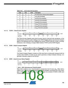
14.11.5 TIMSK – Timer/Counter Interrupt Mask Register
Bit
7
6
5
4
OCIE1A
R/W
0
3
OCIE1B
R/W
0
2
TOIE1
R/W
0
1
OCIE0
R/W
0
0
TOIE0
R/W
0
OCIE2
TOIE2
TICIE1
R/W
0
TIMSK
0x37 (0x57)
Read/Write
Initial Value
R/W
0
R/W
0
• Bit 1 – OCIE0: Timer/Counter0 Output Compare Match Interrupt Enable
When the OCIE0 bit is written to one, and the I-bit in the Status Register is set (one), the
Timer/Counter0 Compare Match interrupt is enabled. The corresponding interrupt is executed if
a Compare Match in Timer/Counter0 occurs, i.e., when the OCF0 bit is set in the Timer/Counter
Interrupt Flag Register – TIFR.
• Bit 0 – TOIE0: Timer/Counter0 Overflow Interrupt Enable
When the TOIE0 bit is written to one, and the I-bit in the Status Register is set (one), the
Timer/Counter0 Overflow interrupt is enabled. The corresponding interrupt is executed if an
overflow in Timer/Counter0 occurs, i.e., when the TOV0 bit is set in the Timer/Counter Interrupt
Flag Register – TIFR.
14.11.6 TIFR – Timer/Counter Interrupt Flag Register
Bit
0x36 (0x56)
7
6
5
4
OCF1A
R/W
0
3
OCF1B
R/W
0
2
TOV1
R/W
0
1
OCF0
R/W
0
0
TOV0
R/W
0
OCF2
TOV2
ICF1
R/W
0
TIFR
Read/Write
Initial Value
R/W
0
R/W
0
• Bit 1 – OCF0: Output Compare Flag 0
The OCF0 bit is set (one) when a Compare Match occurs between the Timer/Counter0 and the
data in OCR0 – Output Compare Register0. OCF0 is cleared by hardware when executing the
corresponding interrupt handling vector. Alternatively, OCF0 is cleared by writing a logic one to
109
8160C–AVR–07/09

 ATMEL [ ATMEL ]