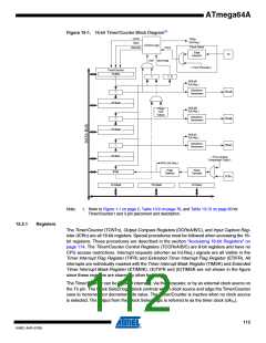
ATmega64A
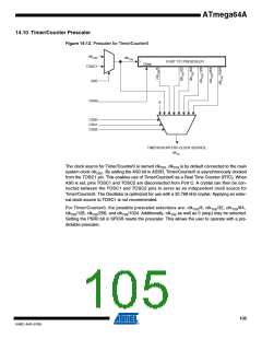
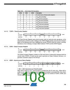
Table 14-6. Clock Select Bit Description
CS02
CS01
CS00
Description
0
0
0
0
1
1
1
1
0
0
1
1
0
0
1
1
0
1
0
1
0
1
0
1
No clock source (Timer/counter stopped)
clkT0S/(No prescaling)
clkT0S/8 (From prescaler)
clkT0S/32 (From prescaler)
clkT0S/64 (From prescaler)
clkT0S/128 (From prescaler)
clkT S/256 (From prescaler)
0
clkT S/1024 (From prescaler)
0
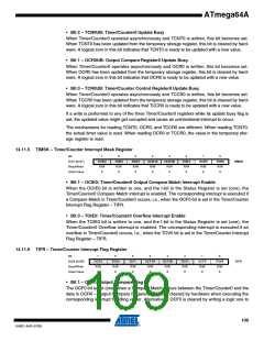
14.11.2 TCNT0 – Timer/Counter Register
Bit
7
6
5
4
3
2
1
0
0x32 (0x52)
Read/Write
Initial Value
TCNT0[7:0]
TCNT0
R/W
0
R/W
0
R/W
0
R/W
0
R/W
0
R/W
0
R/W
0
R/W
0
The Timer/Counter Register gives direct access, both for read and write operations, to the
Timer/Counter unit 8-bit counter. Writing to the TCNT0 Register blocks (removes) the Compare
Match on the following timer clock. Modifying the counter (TCNT0) while the counter is running,
introduces a risk of missing a Compare Match between TCNT0 and the OCR0 Register.
14.11.3 OCR0 – Output Compare Register
Bit
7
6
5
4
3
2
1
0
0x31 (0x51)
Read/Write
Initial Value
OCR0[7:0]
OCR0
R/W
0
R/W
0
R/W
0
R/W
0
R/W
0
R/W
0
R/W
0
R/W
0
The Output Compare Register contains an 8-bit value that is continuously compared with the
counter value (TCNT0). A match can be used to generate an Output Compare interrupt, or to
generate a waveform output on the OC0 pin.
14.11.4 ASSR – Asynchronous Status Register
Bit
0x30 (0x50)
7
6
5
–
4
–
3
2
1
0
–
–
AS0
R/W
0
TCN0UB
OCR0UB
TCR0UB
ASSR
Read/Write
Initial Value
R
0
R
0
R
0
R
0
R
0
R
0
R
0
• Bit 3 – AS0: Asynchronous Timer/Counter0
When AS0 is written to zero, Timer/Counter0 is clocked from the I/O clock, clkI/O. When AS0 is
written to one, Timer/Counter 0 is clocked from a crystal Oscillator connected to the Timer Oscil-
lator 1 (TOSC1) pin. When the value of AS0 is changed, the contents of TCNT0, OCR0, and
TCCR0 might be corrupted.
108
8160C–AVR–07/09

 ATMEL [ ATMEL ]