ATmega48PA/88PA/168PA/328P
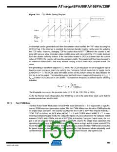
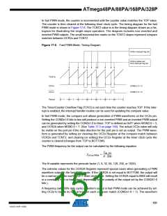
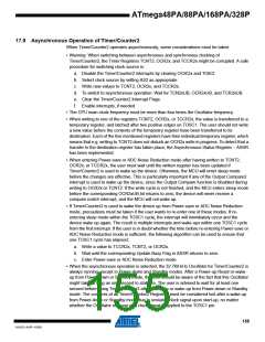
In fast PWM mode, the counter is incremented until the counter value matches the TOP value.
The counter is then cleared at the following timer clock cycle. The timing diagram for the fast
PWM mode is shown in Figure 17-6. The TCNT2 value is in the timing diagram shown as a his-
togram for illustrating the single-slope operation. The diagram includes non-inverted and
inverted PWM outputs. The small horizontal line marks on the TCNT2 slopes represent compare
matches between OCR2x and TCNT2.
Figure 17-6. Fast PWM Mode, Timing Diagram
OCRnx Interrupt Flag Set
OCRnx Update and
TOVn Interrupt Flag Set
TCNTn
(COMnx1:0 = 2)
(COMnx1:0 = 3)
OCnx
OCnx
1
2
3
4
5
6
7
Period
The Timer/Counter Overflow Flag (TOV2) is set each time the counter reaches TOP. If the inter-
rupt is enabled, the interrupt handler routine can be used for updating the compare value.
In fast PWM mode, the compare unit allows generation of PWM waveforms on the OC2x pin.
Setting the COM2x1:0 bits to two will produce a non-inverted PWM and an inverted PWM output
can be generated by setting the COM2x1:0 to three. TOP is defined as 0xFF when WGM2:0 = 3,
and OCR2A when MGM2:0 = 7. (See Table 17-3 on page 158). The actual OC2x value will only
be visible on the port pin if the data direction for the port pin is set as output. The PWM wave-
form is generated by setting (or clearing) the OC2x Register at the compare match between
OCR2x and TCNT2, and clearing (or setting) the OC2x Register at the timer clock cycle the
counter is cleared (changes from TOP to BOTTOM).
The PWM frequency for the output can be calculated by the following equation:
f
clk_I/O
f
= -----------------
OCnxPWM
N ⋅ 256
The N variable represents the prescale factor (1, 8, 32, 64, 128, 256, or 1024).
The extreme values for the OCR2A Register represent special cases when generating a PWM
waveform output in the fast PWM mode. If the OCR2A is set equal to BOTTOM, the output will
be a narrow spike for each MAX+1 timer clock cycle. Setting the OCR2A equal to MAX will result
in a constantly high or low output (depending on the polarity of the output set by the COM2A1:0
bits.)
A frequency (with 50% duty cycle) waveform output in fast PWM mode can be achieved by set-
ting OC2x to toggle its logical level on each compare match (COM2x1:0 = 1). The waveform
151
8161D–AVR–10/09

 ATMEL [ ATMEL ]