ATmega48PA/88PA/168PA/328P
15.5 Counter Unit
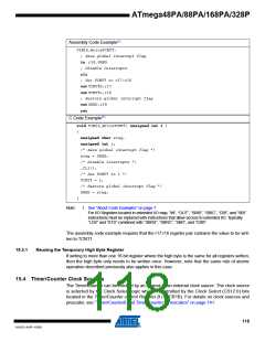
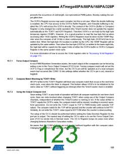
The main part of the 16-bit Timer/Counter is the programmable 16-bit bi-directional counter unit.
Figure 15-2 shows a block diagram of the counter and its surroundings.
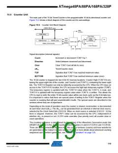
Figure 15-2. Counter Unit Block Diagram
DATA BUS (8-bit)
TOVn
(Int.Req.)
TEMP (8-bit)
Clock Select
Edge
Count
Tn
Detector
TCNTnH (8-bit)
TCNTnL (8-bit)
Clear
clkTn
Control Logic
Direction
TCNTn (16-bit Counter)
( From Prescaler )
TOP
BOTTOM
Signal description (internal signals):
Count
Increment or decrement TCNT1 by 1.
Direction
Clear
Select between increment and decrement.
Clear TCNT1 (set all bits to zero).
clkT
Timer/Counter clock.
1
TOP
Signalize that TCNT1 has reached maximum value.
Signalize that TCNT1 has reached minimum value (zero).
BOTTOM
The 16-bit counter is mapped into two 8-bit I/O memory locations: Counter High (TCNT1H) con-
taining the upper eight bits of the counter, and Counter Low (TCNT1L) containing the lower eight
bits. The TCNT1H Register can only be indirectly accessed by the CPU. When the CPU does an
access to the TCNT1H I/O location, the CPU accesses the high byte temporary register (TEMP).
The temporary register is updated with the TCNT1H value when the TCNT1L is read, and
TCNT1H is updated with the temporary register value when TCNT1L is written. This allows the
CPU to read or write the entire 16-bit counter value within one clock cycle via the 8-bit data bus.
It is important to notice that there are special cases of writing to the TCNT1 Register when the
counter is counting that will give unpredictable results. The special cases are described in the
sections where they are of importance.
Depending on the mode of operation used, the counter is cleared, incremented, or decremented
at each timer clock (clk ). The clk 1 can be generated from an external or internal clock source,
1
T
T
selected by the Clock Select bits (CS12:0). When no clock source is selected (CS12:0 = 0) the
timer is stopped. However, the TCNT1 value can be accessed by the CPU, independent of
whether clkT is present or not. A CPU write overrides (has priority over) all counter clear or
1
count operations.
The counting sequence is determined by the setting of the Waveform Generation mode bits
(WGM13:0) located in the Timer/Counter Control Registers A and B (TCCR1A and TCCR1B).
There are close connections between how the counter behaves (counts) and how waveforms
are generated on the Output Compare outputs OC1x. For more details about advanced counting
sequences and waveform generation, see ”Modes of Operation” on page 125.
119
8161D–AVR–10/09

 ATMEL [ ATMEL ]