ATmega48PA/88PA/168PA/328P
14.7.1
Normal Mode
The simplest mode of operation is the Normal mode (WGM02:0 = 0). In this mode the counting
direction is always up (incrementing), and no counter clear is performed. The counter simply
overruns when it passes its maximum 8-bit value (TOP = 0xFF) and then restarts from the bot-
tom (0x00). In normal operation the Timer/Counter Overflow Flag (TOV0) will be set in the same
timer clock cycle as the TCNT0 becomes zero. The TOV0 Flag in this case behaves like a ninth
bit, except that it is only set, not cleared. However, combined with the timer overflow interrupt
that automatically clears the TOV0 Flag, the timer resolution can be increased by software.
There are no special cases to consider in the Normal mode, a new counter value can be written
anytime.
The Output Compare unit can be used to generate interrupts at some given time. Using the Out-
put Compare to generate waveforms in Normal mode is not recommended, since this will
occupy too much of the CPU time.
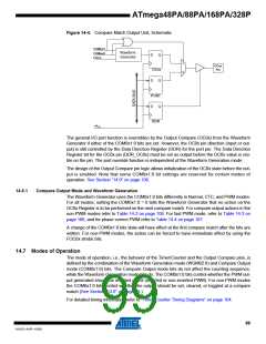
14.7.2
Clear Timer on Compare Match (CTC) Mode
In Clear Timer on Compare or CTC mode (WGM02:0 = 2), the OCR0A Register is used to
manipulate the counter resolution. In CTC mode the counter is cleared to zero when the counter
value (TCNT0) matches the OCR0A. The OCR0A defines the top value for the counter, hence
also its resolution. This mode allows greater control of the compare match output frequency. It
also simplifies the operation of counting external events.
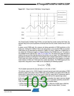
The timing diagram for the CTC mode is shown in Figure 14-5. The counter value (TCNT0)
increases until a compare match occurs between TCNT0 and OCR0A, and then counter
(TCNT0) is cleared.
Figure 14-5. CTC Mode, Timing Diagram
OCnx Interrupt Flag Set
TCNTn
OCn
(Toggle)
(COMnx1:0 = 1)
1
2
3
4
Period
An interrupt can be generated each time the counter value reaches the TOP value by using the
OCF0A Flag. If the interrupt is enabled, the interrupt handler routine can be used for updating
the TOP value. However, changing TOP to a value close to BOTTOM when the counter is run-
ning with none or a low prescaler value must be done with care since the CTC mode does not
have the double buffering feature. If the new value written to OCR0A is lower than the current
value of TCNT0, the counter will miss the compare match. The counter will then have to count to
its maximum value (0xFF) and wrap around starting at 0x00 before the compare match can
occur.
For generating a waveform output in CTC mode, the OC0A output can be set to toggle its logical
level on each compare match by setting the Compare Output mode bits to toggle mode
(COM0A1:0 = 1). The OC0A value will not be visible on the port pin unless the data direction for
100
8161D–AVR–10/09

 ATMEL [ ATMEL ]