ATmega16M1/32M1/64M1
2.1
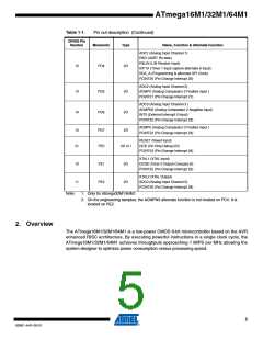
Block Diagram
Figure 2-1. Block Diagram
Data Bus 8-bit
Interrupt
Unit
Program
Counter
Status
and Control
Flash Program
Memory
SPI
Unit
32 x 8
General
Purpose
Registrers
Instruction
Register
Watchdog
Timer
4 Analog
Comparators
Instruction
Decoder
ALU
HW LIN/UART
Timer 0
Timer 1
ADC
Control Lines
Data
SRAM
EEPROM
DAC
MPSC
I/O Lines
CAN
Current Source
The AVR core combines a rich instruction set with 32 general purpose working registers. All the
32 registers are directly connected to the Arithmetic Logic Unit (ALU), allowing two independent
registers to be accessed in one single instruction executed in one clock cycle. The resulting
architecture is more code efficient while achieving throughputs up to ten times faster than con-
ventional CISC microcontrollers.
The ATmega16M1/32M1/64M1 provides the following features: 16/32/64K bytes of In-System
Programmable Flash with Read-While-Write capabilities, 512B/1K/2K bytes EEPROM,
1/2/4K bytes SRAM, 27 general purpose I/O lines, 32 general purpose working registers, one
Motor Power Stage Controller, two flexible Timer/Counters with compare modes and PWM, one
UART with HW LIN, an 11-channel 10-bit ADC with two differential input stages with program-
mable gain, a 10-bit DAC, a programmable Watchdog Timer with Internal Individual Oscillator,
an SPI serial port, an On-chip Debug system and four software selectable power saving modes.
6
8209C–AVR–05/10

 ATMEL [ ATMEL ]