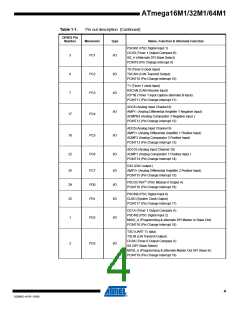
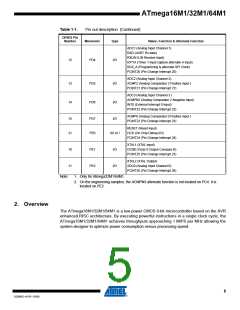
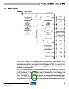
ATmega16M1/32M1/64M1
2.2.5
Port D (PD7..PD0)
Port D is an 8-bit bi-directional I/O port with internal pull-up resistors (selected for each bit). The
Port D output buffers have symmetrical drive characteristics with both high sink and source
capability. As inputs, Port D pins that are externally pulled low will source current if the pull-up
resistors are activated. The Port D pins are tri-stated when a reset condition becomes active,
even if the clock is not running.
Port D also serves the functions of various special features of the ATmega16M1/32M1/64M1 as
listed on page 79.
2.2.6
Port E (PE2..0) RESET/ XTAL1/
XTAL2
Port E is an 3-bit bi-directional I/O port with internal pull-up resistors (selected for each bit). The
Port E output buffers have symmetrical drive characteristics with both high sink and source
capability. As inputs, Port E pins that are externally pulled low will source current if the pull-up
resistors are activated. The Port E pins are tri-stated when a reset condition becomes active,
even if the clock is not running.
If the RSTDISBL Fuse is programmed, PE0 is used as an I/O pin. Note that the electrical char-
acteristics of PE0 differ from those of the other pins of Port E.
If the RSTDISBL Fuse is unprogrammed, PE0 is used as a Reset input. A low level on this pin
for longer than the minimum pulse length will generate a Reset, even if the clock is not running.
The minimum pulse length is given in “System and Reset Characteristics” on page 313. Shorter
pulses are not guaranteed to generate a Reset.
Depending on the clock selection fuse settings, PE1 can be used as input to the inverting Oscil-
lator amplifier and input to the internal clock operating circuit.
Depending on the clock selection fuse settings, PE2 can be used as output from the inverting
Oscillator amplifier.
The various special features of Port E are elaborated in “Alternate Functions of Port E” on page
82 and “Clock Systems and their Distribution” on page 27.
2.2.7
2.2.8
AVCC
AREF
AVCC is the supply voltage pin for the A/D Converter, D/A Converter, Current source. It should
be externally connected to VCC, even if the ADC, DAC are not used. If the ADC is used, it should
be connected to VCC through a low-pass filter.
This is the analog reference pin for the A/D Converter.
8
8209BS–AVR–10/09

 ATMEL [ ATMEL ]