A Flash program corruption can be caused by two situations when the voltage is too low. First, a
regular write sequence to the Flash requires a minimum voltage to operate correctly. Secondly,
the CPU itself can execute instructions incorrectly, if the supply voltage for executing instructions
is too low.
Flash corruption can easily be avoided by following these design recommendations (one is
sufficient):
1. Keep the AVR RESET active (low) during periods of insufficient power supply voltage.
This can be done by enabling the internal Brown-out Detector (BOD) if the operating volt-
age matches the detection level. If not, an external low VCC reset protection circuit can be
used. If a reset occurs while a write operation is in progress, the write operation will be
completed provided that the power supply voltage is sufficient.
2. Keep the AVR core in Power-down sleep mode during periods of low VCC. This will pre-
vent the CPU from attempting to decode and execute instructions, effectively protecting
the SPMCSR Register and thus the Flash from unintentional writes.
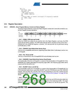
25.2.4
Programming Time for Flash when Using SPM
The calibrated RC Oscillator is used to time Flash accesses. Table 26-5 shows the typical pro-
gramming time for Flash accesses from the CPU.
Table 25-1. SPM Programming Time(1)
Symbol
Min Programming Time
Max Programming Time
Flash write (Page Erase, Page Write, and
write Lock bits by SPM)
3.7 ms
4.5 ms
Note:
1. Minimum and maximum programming time is per individual operation.
25.2.5
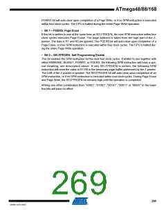
Simple Assembly Code Example for a Boot Loader
Note that the RWWSB bit will always be read as zero in ATmega48. Nevertheless, it is recom-
mended to check this bit as shown in the code example, to ensure compatibility with devices
supporting Read-While-Write.
;-the routine writes one page of data from RAM to Flash
; the first data location in RAM is pointed to by the Y pointer
; the first data location in Flash is pointed to by the Z-pointer
;-error handling is not included
;-the routine must be placed inside the Boot space
; (at least the Do_spm sub routine). Only code inside NRWW section can
; be read during Self-Programming (Page Erase and Page Write).
;-registers used: r0, r1, temp1 (r16), temp2 (r17), looplo (r24),
; loophi (r25), spmcrval (r20)
; storing and restoring of registers is not included in the routine
; register usage can be optimized at the expense of code size
;-It is assumed that either the interrupt table is moved to the Boot
; loader section or that the interrupts are disabled.
.equ PAGESIZEB = PAGESIZE*2
.org SMALLBOOTSTART
Write_page:
;PAGESIZEB is page size in BYTES, not words
; Page Erase
ldi spmcrval, (1<<PGERS) | (1<<SELFPRGEN)
rcallDo_spm
; re-enable the RWW section
ldi spmcrval, (1<<RWWSRE) | (1<<SELFPRGEN)
266
ATmega48/88/168
2545M–AVR–09/07

 ATMEL [ ATMEL ]