ATmega48/88/168
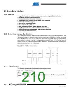
Table 21-1. TWI Terminology
Term
Description
Slave
The device addressed by a Master.
The device placing data on the bus.
The device reading data from the bus.
Transmitter
Receiver
The PRTWI bit in “Minimizing Power Consumption” on page 42 must be written to zero to enable
the 2-wire Serial Interface.
21.2.2
Electrical Interconnection
As depicted in Figure 21-1, both bus lines are connected to the positive supply voltage through
pull-up resistors. The bus drivers of all TWI-compliant devices are open-drain or open-collector.
This implements a wired-AND function which is essential to the operation of the interface. A low
level on a TWI bus line is generated when one or more TWI devices output a zero. A high level
is output when all TWI devices tri-state their outputs, allowing the pull-up resistors to pull the line
high. Note that all AVR devices connected to the TWI bus must be powered in order to allow any
bus operation.
The number of devices that can be connected to the bus is only limited by the bus capacitance
limit of 400 pF and the 7-bit slave address space. A detailed specification of the electrical char-
acteristics of the TWI is given in “2-wire Serial Interface Characteristics” on page 309. Two
different sets of specifications are presented there, one relevant for bus speeds below 100 kHz,
and one valid for bus speeds up to 400 kHz.
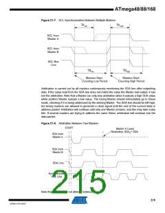
21.3 Data Transfer and Frame Format
21.3.1
Transferring Bits
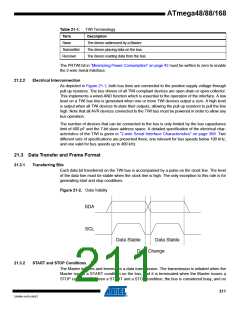
Each data bit transferred on the TWI bus is accompanied by a pulse on the clock line. The level
of the data line must be stable when the clock line is high. The only exception to this rule is for
generating start and stop conditions.
Figure 21-2. Data Validity
SDA
SCL
Data Stable
Data Stable
Data Change
21.3.2
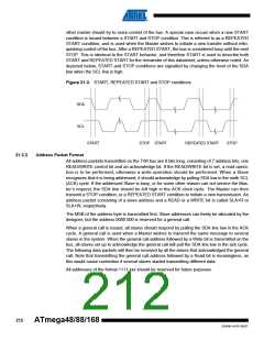
START and STOP Conditions
The Master initiates and terminates a data transmission. The transmission is initiated when the
Master issues a START condition on the bus, and it is terminated when the Master issues a
STOP condition. Between a START and a STOP condition, the bus is considered busy, and no
211
2545M–AVR–09/07

 ATMEL [ ATMEL ]