A FOC2B strobe will not generate any interrupt, nor will it clear the timer in CTC mode using
OCR2B as TOP.
The FOC2B bit is always read as zero.
• Bits 5:4 – Res: Reserved Bits
These bits are reserved bits in the ATmega48/88/168 and will always read as zero.
• Bit 3 – WGM22: Waveform Generation Mode
See the description in the “TCCR2A – Timer/Counter Control Register A” on page 154.
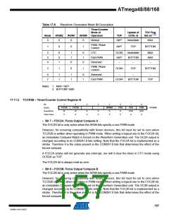
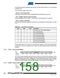
• Bit 2:0 – CS22:0: Clock Select
The three Clock Select bits select the clock source to be used by the Timer/Counter, see Table
17-9.
Table 17-9. Clock Select Bit Description
CS22
CS21
CS20
Description
0
0
0
0
1
1
1
1
0
0
1
1
0
0
1
1
0
1
0
1
0
1
0
1
No clock source (Timer/Counter stopped).
clkT2S/(No prescaling)
clkT2S/8 (From prescaler)
clkT2S/32 (From prescaler)
clkT2S/64 (From prescaler)
clkT2S/128 (From prescaler)
clkT S/256 (From prescaler)
2
clkT S/1024 (From prescaler)
2
If external pin modes are used for the Timer/Counter0, transitions on the T0 pin will clock the
counter even if the pin is configured as an output. This feature allows software control of the
counting.
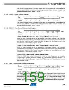
17.11.3 TCNT2 – Timer/Counter Register
Bit
7
6
5
4
3
2
1
0
(0xB2)
TCNT2[7:0]
TCNT2
Read/Write
Initial Value
R/W
0
R/W
0
R/W
0
R/W
0
R/W
0
R/W
0
R/W
0
R/W
0
The Timer/Counter Register gives direct access, both for read and write operations, to the
Timer/Counter unit 8-bit counter. Writing to the TCNT2 Register blocks (removes) the Compare
Match on the following timer clock. Modifying the counter (TCNT2) while the counter is running,
introduces a risk of missing a Compare Match between TCNT2 and the OCR2x Registers.
17.11.4 OCR2A – Output Compare Register A
Bit
7
6
5
4
3
2
1
0
(0xB3)
OCR2A[7:0]
OCR2A
Read/Write
Initial Value
R/W
0
R/W
0
R/W
0
R/W
0
R/W
0
R/W
0
R/W
0
R/W
0
158
ATmega48/88/168
2545M–AVR–09/07

 ATMEL [ ATMEL ]