The clock source for Timer/Counter2 is named clkT2S. clkT2S is by default connected to the main
system I/O clock clkIO. By setting the AS2 bit in ASSR, Timer/Counter2 is asynchronously
clocked from the TOSC1 pin. This enables use of Timer/Counter2 as a Real Time Counter
(RTC). When AS2 is set, pins TOSC1 and TOSC2 are disconnected from Port C. A crystal can
then be connected between the TOSC1 and TOSC2 pins to serve as an independent clock
source for Timer/Counter2. The Oscillator is optimized for use with a 32.768 kHz crystal.
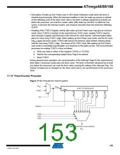
For Timer/Counter2, the possible prescaled selections are: clkT2S/8, clkT2S/32, clkT2S/64,
clkT2S/128, clkT2S/256, and clkT2S/1024. Additionally, clkT2S as well as 0 (stop) may be selected.
Setting the PSRASY bit in GTCCR resets the prescaler. This allows the user to operate with a
predictable prescaler.
17.11 Register Description
17.11.1 TCCR2A – Timer/Counter Control Register A
Bit
7
COM2A1
R/W
6
COM2A0
R/W
5
COM2B1
R/W
4
COM2B0
R/W
3
–
2
–
1
WGM21
R/W
0
0
WGM20
R/W
0
TCCR2A
(0xB0)
Read/Write
Initial Value
R
0
R
0
0
0
0
0
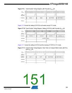
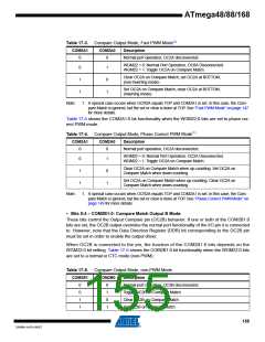
• Bits 7:6 – COM2A1:0: Compare Match Output A Mode
These bits control the Output Compare pin (OC2A) behavior. If one or both of the COM2A1:0
bits are set, the OC2A output overrides the normal port functionality of the I/O pin it is connected
to. However, note that the Data Direction Register (DDR) bit corresponding to the OC2A pin
must be set in order to enable the output driver.
When OC2A is connected to the pin, the function of the COM2A1:0 bits depends on the
WGM22:0 bit setting. Table 17-2 shows the COM2A1:0 bit functionality when the WGM22:0 bits
are set to a normal or CTC mode (non-PWM).
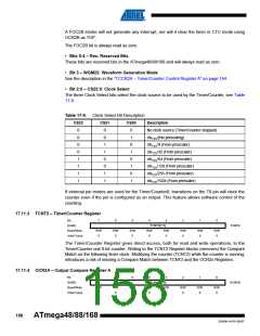
Table 17-2. Compare Output Mode, non-PWM Mode
COM2A1
COM2A0
Description
0
0
1
1
0
1
0
1
Normal port operation, OC2A disconnected.
Toggle OC2A on Compare Match
Clear OC2A on Compare Match
Set OC2A on Compare Match
Table 17-3 on page 155 shows the COM2A1:0 bit functionality when the WGM21:0 bits are set
to fast PWM mode.
154
ATmega48/88/168
2545M–AVR–09/07

 ATMEL [ ATMEL ]