8-bit
Timer/Counter
Register
Description
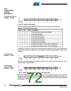
Timer/Counter Control
Register – TCCR0
Bit
7
–
6
–
5
–
4
–
3
–
2
CS02
R/W
0
1
CS01
R/W
0
0
CS00
R/W
0
TCCR0
Read/Write
Initial Value
R
0
R
0
R
0
R
0
R
0
• Bit 2:0 – CS02:0: Clock Select
The three clock select bits select the clock source to be used by the Timer/Counter.
Table 34. Clock Select Bit Description
CS02
CS01
CS00
Description
0
0
0
0
1
1
1
1
0
0
1
1
0
0
1
1
0
1
0
1
0
1
0
1
No clock source (Timer/Counter stopped).
clkI/O/(No prescaling)
clkI/O/8 (From prescaler)
clkI/O/64 (From prescaler)
clkI/O/256 (From prescaler)
clkI/O/1024 (From prescaler)
External clock source on T0 pin. Clock on falling edge.
External clock source on T0 pin. Clock on rising edge.
If external pin modes are used for the Timer/Counter0, transitions on the T0 pin will clock the
counter even if the pin is configured as an output. This feature allows software control of the
counting.
Timer/Counter
Register – TCNT0
Bit
7
6
5
4
3
2
1
0
TCNT0[7:0]
TCNT0
Read/Write
Initial Value
R/W
0
R/W
0
R/W
0
R/W
0
R/W
0
R/W
0
R/W
0
R/W
0
The Timer/Counter Register gives direct access, both for read and write operations, to the
Timer/Counter unit 8-bit counter.
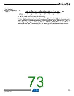
Timer/Counter
Interrupt Mask
Register – TIMSK
Bit
7
OCIE2
R/W
0
6
TOIE2
R/W
0
5
TICIE1
R/W
0
4
OCIE1A
R/W
0
3
OCIE1B
R/W
0
2
TOIE1
R/W
0
1
–
0
TOIE0
R/W
0
TIMSK
Read/Write
Initial Value
R/W
0
• Bit 0 – TOIE0: Timer/Counter0 Overflow Interrupt Enable
When the TOIE0 bit is written to one, and the I-bit in the Status Register is set (one), the
Timer/Counter0 Overflow interrupt is enabled. The corresponding interrupt is executed if an
overflow in Timer/Counter0 occurs, i.e., when the TOV0 bit is set in the Timer/Counter Interrupt
Flag Register – TIFR.
72
ATmega8(L)
2486T–AVR–05/08

 ATMEL [ ATMEL ]