ATmega8(L)
Serial Programming
Algorithm
When writing serial data to the ATmega8, data is clocked on the rising edge of SCK.
When reading data from the ATmega8, data is clocked on the falling edge of SCK. See Figure
113 on page 232 for timing details.
To program and verify the ATmega8 in the Serial Programming mode, the following sequence is
recommended (see four byte instruction formats in Table 98 on page 233):
1. Power-up sequence:
Apply power between VCC and GND while RESET and SCK are set to “0”. In some sys-
tems, the programmer can not guarantee that SCK is held low during Power-up. In this
case, RESET must be given a positive pulse of at least two CPU clock cycles duration
after SCK has been set to “0”
2. Wait for at least 20ms and enable Serial Programming by sending the Programming
Enable serial instruction to pin MOSI
3. The Serial Programming instructions will not work if the communication is out of synchro-
nization. When in sync. the second byte (0x53), will echo back when issuing the third
byte of the Programming Enable instruction. Whether the echo is correct or not, all four
bytes of the instruction must be transmitted. If the 0x53 did not echo back, give RESET a
positive pulse and issue a new Programming Enable command
4. The Flash is programmed one page at a time. The page size is found in Table 89 on
page 218. The memory page is loaded one byte at a time by supplying the 5 LSB of the
address and data together with the Load Program memory Page instruction. To ensure
correct loading of the page, the data Low byte must be loaded before data High byte is
applied for a given address. The Program memory Page is stored by loading the Write
Program memory Page instruction with the 7MSB of the address. If polling is not used,
the user must wait at least tWD_FLASH before issuing the next page (see Table 97 on page
232).
Note: If other commands than polling (read) are applied before any write operation (FLASH,
EEPROM, Lock Bits, Fuses) is completed, it may result in incorrect programming
5. The EEPROM array is programmed one byte at a time by supplying the address and data
together with the appropriate Write instruction. An EEPROM memory location is first
automatically erased before new data is written. If polling is not used, the user must wait
at least tWD_EEPROM before issuing the next byte (see Table 97 on page 232). In a chip
erased device, no 0xFFs in the data file(s) need to be programmed
6. Any memory location can be verified by using the Read instruction which returns the con-
tent at the selected address at serial output MISO
7. At the end of the programming session, RESET can be set high to commence normal
operation
8. Power-off sequence (if needed):
Set RESET to “1”
Turn VCC power off
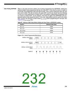
Data Polling Flash
When a page is being programmed into the Flash, reading an address location within the page
being programmed will give the value 0xFF. At the time the device is ready for a new page, the
programmed value will read correctly. This is used to determine when the next page can be writ-
ten. Note that the entire page is written simultaneously and any address within the page can be
used for polling. Data polling of the Flash will not work for the value 0xFF, so when programming
this value, the user will have to wait for at least tWD_FLASH before programming the next page. As
a chip-erased device contains 0xFF in all locations, programming of addresses that are meant to
contain 0xFF, can be skipped. See Table 97 on page 232 for tWD_FLASH value.
231
2486AA–AVR–02/2013

 ATMEL [ ATMEL ]