ATmega8(L)
Serial
Downloading
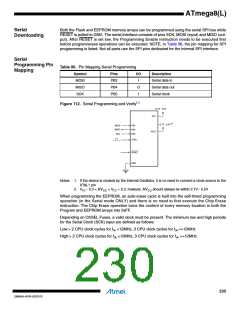
Both the Flash and EEPROM memory arrays can be programmed using the serial SPI bus while
RESET is pulled to GND. The serial interface consists of pins SCK, MOSI (input) and MISO (out-
put). After RESET is set low, the Programming Enable instruction needs to be executed first
before program/erase operations can be executed. NOTE, in Table 96, the pin mapping for SPI
programming is listed. Not all parts use the SPI pins dedicated for the internal SPI interface.
Serial
Programming Pin
Mapping
Table 96. Pin Mapping Serial Programming
Symbol
MOSI
MISO
SCK
Pins
PB3
PB4
PB5
I/O
Description
Serial data in
Serial data out
Serial clock
I
O
I
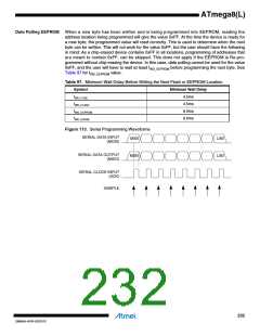
Figure 112. Serial Programming and Verify(1)
+2.7V - 5.5V
VCC
+2.7V - 5.5V (2)
MOSI
MISO
PB3
PB4
PB5
AVCC
SCK
XTAL1
RESET
GND
Notes: 1. If the device is clocked by the Internal Oscillator, it is no need to connect a clock source to the
XTAL1 pin
2. VCC - 0.3 < AVCC < VCC + 0.3, however, AVCC should always be within 2.7V - 5.5V
When programming the EEPROM, an auto-erase cycle is built into the self-timed programming
operation (in the Serial mode ONLY) and there is no need to first execute the Chip Erase
instruction. The Chip Erase operation turns the content of every memory location in both the
Program and EEPROM arrays into 0xFF.
Depending on CKSEL Fuses, a valid clock must be present. The minimum low and high periods
for the Serial Clock (SCK) input are defined as follows:
Low:> 2 CPU clock cycles for fck <12MHz, 3 CPU clock cycles for fck >=12MHz
High:> 2 CPU clock cycles for fck <12MHz, 3 CPU clock cycles for fck >=12MHz
230
2486AA–AVR–02/2013

 ATMEL [ ATMEL ]