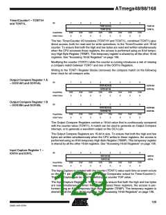
ATmega48/88/168
operation is controlled by the Asynchronous Status Register (ASSR). The Clock Select
logic block controls which clock source he Timer/Counter uses to increment (or decre-
ment) its value. The Timer/Counter is inactive when no clock source is selected. The
output from the Clock Select logic is referred to as the timer clock (clkT2).
The double buffered Output Compare Register (OCR2A and OCR2B) are compared
with the Timer/Counter value at all times. The result of the compare can be used by the
Waveform Generator to generate a PWM or variable frequency output on the Output
Compare pins (OC2A and OC2B). See “Output Compare Unit” on page 134. for details.
The compare match event will also set the Compare Flag (OCF2A or OCF2B) which can
be used to generate an Output Compare interrupt request.
Definitions
Many register and bit references in this document are written in general form. A lower
case “n” replaces the Timer/Counter number, in this case 2. However, when using the
register or bit defines in a program, the precise form must be used, i.e., TCNT2 for
accessing Timer/Counter2 counter value and so on.
The definitions in Table 59 are also used extensively throughout the section.
Table 59. Definitions
BOTTOM The counter reaches the BOTTOM when it becomes zero (0x00).
MAX
TOP
The counter reaches its MAXimum when it becomes 0xFF (decimal 255).
The counter reaches the TOP when it becomes equal to the highest
value in the count sequence. The TOP value can be assigned to be the
fixed value 0xFF (MAX) or the value stored in the OCR2A Register. The
assignment is dependent on the mode of operation.
Timer/Counter Clock
Sources
The Timer/Counter can be clocked by an internal synchronous or an external asynchro-
nous clock source. The clock source clkT2 is by default equal to the MCU clock, clkI/O.
When the AS2 bit in the ASSR Register is written to logic one, the clock source is taken
from the Timer/Counter Oscillator connected to TOSC1 and TOSC2. For details on
asynchronous operation, see “Asynchronous Status Register – ASSR” on page 150. For
details on clock sources and prescaler, see “Timer/Counter Prescaler” on page 152.
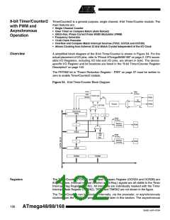
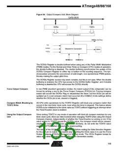
Counter Unit
The main part of the 8-bit Timer/Counter is the programmable bi-directional counter unit.
Figure 55 shows a block diagram of the counter and its surrounding environment.
Figure 55. Counter Unit Block Diagram
TOVn
(Int.Req.)
DATA BUS
TOSC1
count
T/C
Oscillator
clk Tn
clear
TCNTn
Control Logic
Prescaler
direction
TOSC2
clk
bottom
top
I/O
Signal description (internal signals):
count Increment or decrement TCNT2 by 1.
direction Selects between increment and decrement.
133
2545D–AVR–07/04

 ATMEL [ ATMEL ]