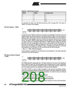
Table 90. TWI Bit Rate Prescaler
TWPS1
TWPS0
Prescaler Value
0
0
1
1
0
1
0
1
1
4
16
64
To calculate bit rates, see “Bit Rate Generator Unit” on page 204. The value of
TWPS1..0 is used in the equation.
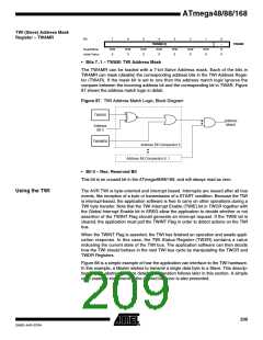
TWI Data Register – TWDR
Bit
7
TWD7
R/W
1
6
TWD6
R/W
1
5
TWD5
R/W
1
4
TWD4
R/W
1
3
TWD3
R/W
1
2
TWD2
R/W
1
1
TWD1
R/W
1
0
TWD0
R/W
1
TWDR
Read/Write
Initial Value
In Transmit mode, TWDR contains the next byte to be transmitted. In Receive mode, the
TWDR contains the last byte received. It is writable while the TWI is not in the process of
shifting a byte. This occurs when the TWI Interrupt Flag (TWINT) is set by hardware.
Note that the Data Register cannot be initialized by the user before the first interrupt
occurs. The data in TWDR remains stable as long as TWINT is set. While data is shifted
out, data on the bus is simultaneously shifted in. TWDR always contains the last byte
present on the bus, except after a wake up from a sleep mode by the TWI interrupt. In
this case, the contents of TWDR is undefined. In the case of a lost bus arbitration, no
data is lost in the transition from Master to Slave. Handling of the ACK bit is controlled
automatically by the TWI logic, the CPU cannot access the ACK bit directly.
• Bits 7..0 – TWD: TWI Data Register
These eight bits constitute the next data byte to be transmitted, or the latest data byte
received on the 2-wire Serial Bus.
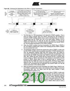
TWI (Slave) Address Register
– TWAR
Bit
7
TWA6
R/W
1
6
TWA5
R/W
1
5
TWA4
R/W
1
4
TWA3
R/W
1
3
TWA2
R/W
1
2
TWA1
R/W
1
1
TWA0
R/W
1
0
TWGCE
R/W
0
TWAR
Read/Write
Initial Value
The TWAR should be loaded with the 7-bit Slave address (in the seven most significant
bits of TWAR) to which the TWI will respond when programmed as a Slave Transmitter
or Receiver, and not needed in the Master modes. In multi master systems, TWAR must
be set in masters which can be addressed as Slaves by other Masters.
The LSB of TWAR is used to enable recognition of the general call address (0x00).
There is an associated address comparator that looks for the slave address (or general
call address if enabled) in the received serial address. If a match is found, an interrupt
request is generated.
• Bits 7..1 – TWA: TWI (Slave) Address Register
These seven bits constitute the slave address of the TWI unit.
• Bit 0 – TWGCE: TWI General Call Recognition Enable Bit
If set, this bit enables the recognition of a General Call given over the 2-wire Serial Bus.
208
ATmega48/88/168
2545D–AVR–07/04

 ATMEL [ ATMEL ]