ATmega48/88/168
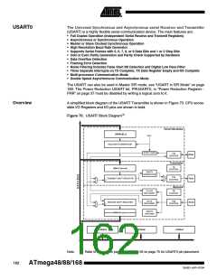
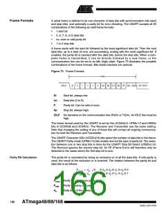
The dashed boxes in the block diagram separate the three main parts of the USART
(listed from the top): Clock Generator, Transmitter and Receiver. Control Registers are
shared by all units. The Clock Generation logic consists of synchronization logic for
external clock input used by synchronous slave operation, and the baud rate generator.
The XCKn (Transfer Clock) pin is only used by synchronous transfer mode. The Trans-
mitter consists of a single write buffer, a serial Shift Register, Parity Generator and
Control logic for handling different serial frame formats. The write buffer allows a contin-
uous transfer of data without any delay between frames. The Receiver is the most
complex part of the USART module due to its clock and data recovery units. The recov-
ery units are used for asynchronous data reception. In addition to the recovery units, the
Receiver includes a Parity Checker, Control logic, a Shift Register and a two level
receive buffer (UDRn). The Receiver supports the same frame formats as the Transmit-
ter, and can detect Frame Error, Data OverRun and Parity Errors.
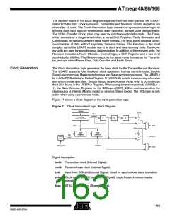
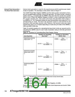
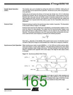
Clock Generation
The Clock Generation logic generates the base clock for the Transmitter and Receiver.
The USART supports four modes of clock operation: Normal asynchronous, Double
Speed asynchronous, Master synchronous and Slave synchronous mode. The UMSELn
bit in USART Control and Status Register C (UCSRnC) selects between asynchronous
and synchronous operation. Double Speed (asynchronous mode only) is controlled by
the U2Xn found in the UCSRnA Register. When using synchronous mode (UMSELn =
1), the Data Direction Register for the XCKn pin (DDR_XCKn) controls whether the
clock source is internal (Master mode) or external (Slave mode). The XCKn pin is only
active when using synchronous mode.
Figure 71 shows a block diagram of the clock generation logic.
Figure 71. Clock Generation Logic, Block Diagram
UBRRn
U2Xn
foscn
UBRRn+1
Prescaling
Down-Counter
/2
/4
/2
0
1
0
1
OSC
txclk
UMSELn
rxclk
DDR_XCKn
Sync
Register
Edge
Detector
xcki
0
1
XCKn
Pin
xcko
DDR_XCKn
UCPOLn
1
0
Signal description:
txclk Transmitter clock (Internal Signal).
rxclk Receiver base clock (Internal Signal).
xcki
Input from XCK pin (internal Signal). Used for synchronous slave operation.
xcko Clock output to XCK pin (Internal Signal). Used for synchronous master
operation.
fosc
XTAL pin frequency (System Clock).
163
2545D–AVR–07/04

 ATMEL [ ATMEL ]