ATmega48/88/168
Serial Peripheral
Interface – SPI
The Serial Peripheral Interface (SPI) allows high-speed synchronous data transfer
between the ATmega48/88/168 and peripheral devices or between several AVR
devices. The ATmega48/88/168 SPI includes the following features:
• Full-duplex, Three-wire Synchronous Data Transfer
• Master or Slave Operation
• LSB First or MSB First Data Transfer
• Seven Programmable Bit Rates
• End of Transmission Interrupt Flag
• Write Collision Flag Protection
• Wake-up from Idle Mode
• Double Speed (CK/2) Master SPI Mode
The USART can also be used in Master SPI mode, see “USART in SPI Mode” on page
189. The PRSPI bit in “Power Reduction Register - PRR” on page 37 must be written to
zero to enable SPI module.
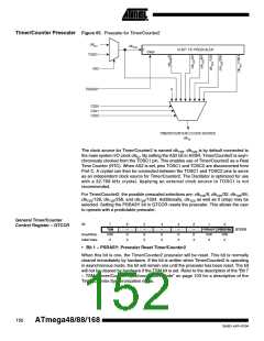
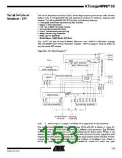
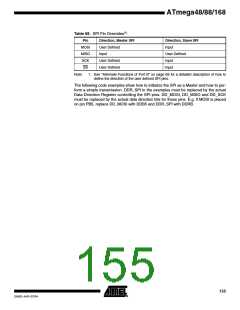
Figure 66. SPI Block Diagram(1)
DIVIDER
/2/4/8/16/32/64/128
Note:
1. Refer to Figure 1 on page 2, and Table 33 on page 69 for SPI pin placement.
The interconnection between Master and Slave CPUs with SPI is shown in Figure 67.
The system consists of two shift Registers, and a Master clock generator. The SPI Mas-
ter initiates the communication cycle when pulling low the Slave Select SS pin of the
desired Slave. Master and Slave prepare the data to be sent in their respective shift
Registers, and the Master generates the required clock pulses on the SCK line to inter-
change data. Data is always shifted from Master to Slave on the Master Out – Slave In,
MOSI, line, and from Slave to Master on the Master In – Slave Out, MISO, line. After
153
2545D–AVR–07/04

 ATMEL [ ATMEL ]