Timer/Counter2 Registers must be considered lost after a wake-up from Power-
down or Standby mode due to unstable clock signal upon start-up, no matter
whether the Oscillator is in use or a clock signal is applied to the TOSC1 pin.
•
•
Description of wake up from Power-save or ADC Noise Reduction mode when the
timer is clocked asynchronously: When the interrupt condition is met, the wake up
process is started on the following cycle of the timer clock, that is, the timer is
always advanced by at least one before the processor can read the counter value.
After wake-up, the MCU is halted for four cycles, it executes the interrupt routine,
and resumes execution from the instruction following SLEEP.
Reading of the TCNT2 Register shortly after wake-up from Power-save may give an
incorrect result. Since TCNT2 is clocked on the asynchronous TOSC clock, reading
TCNT2 must be done through a register synchronized to the internal I/O clock
domain. Synchronization takes place for every rising TOSC1 edge. When waking up
from Power-save mode, and the I/O clock (clkI/O) again becomes active, TCNT2 will
read as the previous value (before entering sleep) until the next rising TOSC1 edge.
The phase of the TOSC clock after waking up from Power-save mode is essentially
unpredictable, as it depends on the wake-up time. The recommended procedure for
reading TCNT2 is thus as follows:
1. Write any value to either of the registers OCR2x or TCCR2x.
2. Wait for the corresponding Update Busy Flag to be cleared.
3. Read TCNT2.
During asynchronous operation, the synchronization of the Interrupt Flags for the asyn-
chronous timer takes 3 processor cycles plus one timer cycle. The timer is therefore
advanced by at least one before the processor can read the timer value causing the set-
ting of the Interrupt Flag. The Output Compare pin is changed on the timer clock and is
not synchronized to the processor clock.
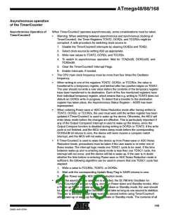
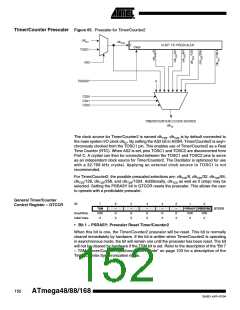
Asynchronous Status
Register – ASSR
Bit
7
–
6
EXCLK
R/W
0
5
4
3
2
1
0
AS2
R/W
0
TCN2UB
OCR2AUB
OCR2BUB
TCR2AUB
TCR2BUB
ASSR
Read/Write
Initial Value
R
0
R
0
R
0
R
0
R
0
R
0
• Bit 6 – EXCLK: Enable External Clock Input
When EXCLK is written to one, and asynchronous clock is selected, the external clock
input buffer is enabled and an external clock can be input on Timer Oscillator 1 (TOSC1)
pin instead of a 32 kHz crystal. Writing to EXCLK should be done before asynchronous
operation is selected. Note that the crystal Oscillator will only run when this bit is zero.
• Bit 5 – AS2: Asynchronous Timer/Counter2
When AS2 is written to zero, Timer/Counter2 is clocked from the I/O clock, clkI/O. When
AS2 is written to one, Timer/Counter2 is clocked from a crystal Oscillator connected to
the Timer Oscillator 1 (TOSC1) pin. When the value of AS2 is changed, the contents of
TCNT2, OCR2A, OCR2B, TCCR2A and TCCR2B might be corrupted.
• Bit 4 – TCN2UB: Timer/Counter2 Update Busy
When Timer/Counter2 operates asynchronously and TCNT2 is written, this bit becomes
set. When TCNT2 has been updated from the temporary storage register, this bit is
cleared by hardware. A logical zero in this bit indicates that TCNT2 is ready to be
updated with a new value.
150
ATmega48/88/168
2545D–AVR–07/04

 ATMEL [ ATMEL ]