determined by the new TOP value. When these two values differ the two slopes of the
period will differ in length. The difference in length gives the unsymmetrical result on the
output.
It is recommended to use the phase and frequency correct mode instead of the phase
correct mode when changing the TOP value while the Timer/Counter is running. When
using a static TOP value there are practically no differences between the two modes of
operation.
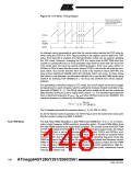
In phase correct PWM mode, the compare units allow generation of PWM waveforms on
the OCnx pins. Setting the COMnx1:0 bits to two will produce a non-inverted PWM and
an inverted PWM output can be generated by setting the COMnx1:0 to three (See Table
81 on page 159). The actual OCnx value will only be visible on the port pin if the data
direction for the port pin is set as output (DDR_OCnx). The PWM waveform is gener-
ated by setting (or clearing) the OCnx Register at the compare match between OCRnx
and TCNTn when the counter increments, and clearing (or setting) the OCnx Register at
compare match between OCRnx and TCNTn when the counter decrements. The PWM
frequency for the output when using phase correct PWM can be calculated by the fol-
lowing equation:
f
clk_I/O
f
= ---------------------------
OCnxPCPWM
2 ⋅ N ⋅ TOP
The N variable represents the prescaler divider (1, 8, 64, 256, or 1024).
The extreme values for the OCRnx Register represent special cases when generating a
PWM waveform output in the phase correct PWM mode. If the OCRnx is set equal to
BOTTOM the output will be continuously low and if set equal to TOP the output will be
continuously high for non-inverted PWM mode. For inverted PWM the output will have
the opposite logic values. If OCR1A is used to define the TOP value (WGM13:0 = 11)
and COM1A1:0 = 1, the OC1A output will toggle with a 50ꢀ duty cycle.
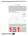
Phase and Frequency Correct The phase and frequency correct Pulse Width Modulation, or phase and frequency cor-
PWM Mode
rect PWM mode (WGMn3:0 = 8 or 9) provides a high resolution phase and frequency
correct PWM waveform generation option. The phase and frequency correct PWM
mode is, like the phase correct PWM mode, based on a dual-slope operation. The
counter counts repeatedly from BOTTOM (0x0000) to TOP and then from TOP to BOT-
TOM. In non-inverting Compare Output mode, the Output Compare (OCnx) is cleared
on the compare match between TCNTn and OCRnx while upcounting, and set on the
compare match while downcounting. In inverting Compare Output mode, the operation
is inverted. The dual-slope operation gives a lower maximum operation frequency com-
pared to the single-slope operation. However, due to the symmetric feature of the dual-
slope PWM modes, these modes are preferred for motor control applications.
The main difference between the phase correct, and the phase and frequency correct
PWM mode is the time the OCRnx Register is updated by the OCRnx Buffer Register,
(see Figure 56 and Figure 57).
The PWM resolution for the phase and frequency correct PWM mode can be defined by
either ICRn or OCRnA. The minimum resolution allowed is 2-bit (ICRn or OCRnA set to
0x0003), and the maximum resolution is 16-bit (ICRn or OCRnA set to MAX). The PWM
resolution in bits can be calculated using the following equation:
log(TOP + 1)
R
= ----------------------------------
PFCPWM
log(2)
152
ATmega640/1280/1281/2560/2561
2549A–AVR–03/05

 ATMEL [ ATMEL ]