ATmega16(L)
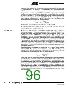
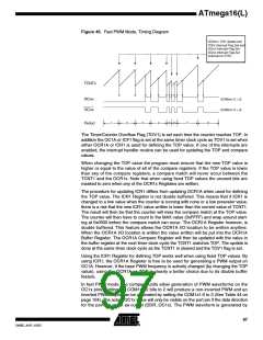
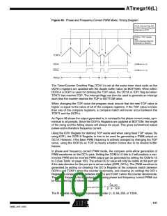
Figure 46. Fast PWM Mode, Timing Diagram
OCRnx / TOP Update and
TOVn Interrupt Flag Set and
OCnA Interrupt Flag Set
OCnA Interrupt Flag Set
(Interrupt on TOP)
TCNTn
(COMnx1:0 = 2)
(COMnx1:0 = 3)
OCnx
OCnx
1
2
3
4
5
6
7
8
Period
The Timer/Counter Overflow Flag (TOV1) is set each time the counter reaches TOP. In
addition the OC1A or ICF1 flag is set at the same timer clock cycle as TOV1 is set when
either OCR1A or ICR1 is used for defining the TOP value. If one of the interrupts are
enabled, the interrupt handler routine can be used for updating the TOP and compare
values.
When changing the TOP value the program must ensure that the new TOP value is
higher or equal to the value of all of the compare registers. If the TOP value is lower
than any of the compare registers, a compare match will never occur between the
TCNT1 and the OCR1x. Note that when using fixed TOP values the unused bits are
masked to zero when any of the OCR1x Registers are written.
The procedure for updating ICR1 differs from updating OCR1A when used for defining
the TOP value. The ICR1 Register is not double buffered. This means that if ICR1 is
changed to a low value when the counter is running with none or a low prescaler value,
there is a risk that the new ICR1 value written is lower than the current value of TCNT1.
The result will then be that the counter will miss the compare match at the TOP value.
The counter will then have to count to the MAX value (0xFFFF) and wrap around start-
ing at 0x0000 before the compare match can occur. The OCR1A Register however, is
double buffered. This feature allows the OCR1A I/O location to be written anytime.
When the OCR1A I/O location is written the value written will be put into the OCR1A
Buffer Register. The OCR1A Compare Register will then be updated with the value in
the buffer register at the next timer clock cycle the TCNT1 matches TOP. The update is
done at the same timer clock cycle as the TCNT1 is cleared and the TOV1 flag is set.
Using the ICR1 Register for defining TOP works well when using fixed TOP values. By
using ICR1, the OCR1A Register is free to be used for generating a PWM output on
OC1A. However, if the base PWM frequency is actively changed (by changing the TOP
value), using the OCR1A as TOP is clearly a better choice due to its double buffer
feature.
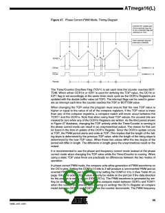
In fast PWM mode, the compare units allow generation of PWM waveforms on the
OC1x pins. Setting the COM1x1:0 bits to 2 will produce a non-inverted PWM and an
inverted PWM output can be generated by setting the COM1x1:0 to 3 (See Table 44 on
page 104). The actual OC1x value will only be visible on the port pin if the data direction
for the port pin is set as output (DDR_OC1x). The PWM waveform is generated by
97
2466E–AVR–10/02

 ATMEL [ ATMEL ]