ATmega16(L)
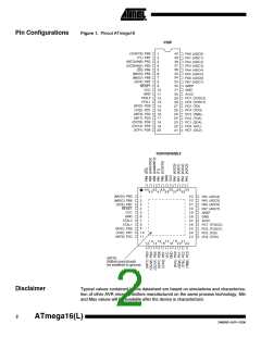
Port B (PB7..PB0)
Port B is an 8-bit bi-directional I/O port with internal pull-up resistors (selected for each
bit). The Port B output buffers have symmetrical drive characteristics with both high sink
and source capability. As inputs, Port B pins that are externally pulled low will source
current if the pull-up resistors are activated. The Port B pins are tri-stated when a reset
condition becomes active, even if the clock is not running.
Port B also serves the functions of various special features of the ATmega16 as listed
on page 56.
Port C (PC7..PC0)
Port C is an 8-bit bi-directional I/O port with internal pull-up resistors (selected for each
bit). The Port C output buffers have symmetrical drive characteristics with both high sink
and source capability. As inputs, Port C pins that are externally pulled low will source
current if the pull-up resistors are activated. The Port C pins are tri-stated when a reset
condition becomes active, even if the clock is not running. If the JTAG interface is
enabled, the pull-up resistors on pins PC5(TDI), PC3(TMS) and PC2(TCK) will be acti-
vated even if a reset occurs.
Port C also serves the functions of the JTAG interface and other special features of the
ATmega16 as listed on page 59.
Port D (PD7..PD0)
Port D is an 8-bit bi-directional I/O port with internal pull-up resistors (selected for each
bit). The Port D output buffers have symmetrical drive characteristics with both high sink
and source capability. As inputs, Port D pins that are externally pulled low will source
current if the pull-up resistors are activated. The Port D pins are tri-stated when a reset
condition becomes active, even if the clock is not running.
Port D also serves the functions of various special features of the ATmega16 as listed
on page 61.
RESET
Reset Input. A low level on this pin for longer than the minimum pulse length will gener-
ate a reset, even if the clock is not running. The minimum pulse length is given in Table
15 on page 36. Shorter pulses are not guaranteed to generate a reset.
XTAL1
XTAL2
AVCC
Input to the inverting Oscillator amplifier and input to the internal clock operating circuit.
Output from the inverting Oscillator amplifier.
AVCC is the supply voltage pin for Port A and the A/D Converter. It should be externally
connected to VCC, even if the ADC is not used. If the ADC is used, it should be con-
nected to VCC through a low-pass filter.
AREF
AREF is the analog reference pin for the A/D Converter.
Resources
A comprehensive set of development tools, application notes and datasheets are avail-
able for download on http://www.atmel.com/avr.
5
2466NS–AVR–10/06

 ATMEL [ ATMEL ]