ATmega169P
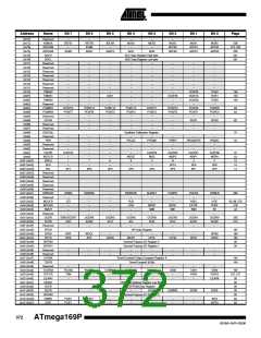
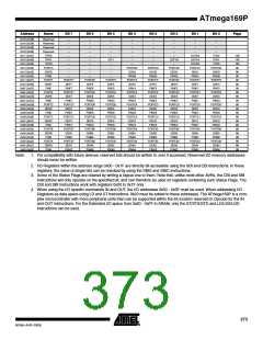
Address
Name
Bit 7
Bit 6
Bit 5
Bit 4
Bit 3
Bit 2
Bit 1
Bit 0
Page
0x1B (0x3B)
0x1A (0x3A)
0x19 (0x39)
0x18 (0x38)
0x17 (0x37)
0x16 (0x36)
0x15 (0x35)
0x14 (0x34)
0x13 (0x33)
0x12 (0x32)
0x11 (0x31)
0x10 (0x30)
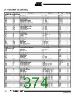
0x0F (0x2F)
0x0E (0x2E)
0x0D (0x2D)
0x0C (0x2C)
0x0B (0x2B)
0x0A (0x2A)
0x09 (0x29)
0x08 (0x28)
0x07 (0x27)
0x06 (0x26)
0x05 (0x25)
0x04 (0x24)
0x03 (0x23)
0x02 (0x22)
0x01 (0x21)
0x00 (0x20)
Reserved
Reserved
Reserved
Reserved
TIFR2
–
–
–
–
–
–
–
–
–
–
–
–
–
–
–
–
–
–
–
–
–
–
–
–
–
–
–
–
–
–
–
–
–
–
–
–
–
–
OCF2A
OCF1A
OCF0A
PORTG1
DDG1
PING1
PORTF1
DDF1
TOV2
TOV1
TOV0
PORTG0
DDG0
PING0
PORTF0
DDF0
PINF0
PORTE0
DDE0
PINE0
PORTD0
DDD0
PIND0
PORTC0
DDC0
PINC0
PORTB0
DDB0
PINB0
PORTA0
DDA0
PINA0
156
134
105
90
90
90
90
90
90
89
89
90
89
89
89
89
89
89
88
88
88
88
88
88
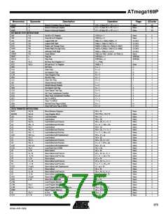
TIFR1
–
–
ICF1
–
–
–
OCF1B
–
TIFR0
–
–
–
–
PORTG
DDRG
PING
–
–
–
PORTG4
DDG4
PING4
PORTF4
DDF4
PINF4
PORTE4
DDE4
PINE4
PORTD4
DDD4
PIND4
PORTC4
DDC4
PINC4
PORTB4
DDB4
PINB4
PORTA4
DDA4
PINA4
PORTG3
DDG3
PING3
PORTF3
DDF3
PINF3
PORTE3
DDE3
PINE3
PORTD3
DDD3
PIND3
PORTC3
DDC3
PINC3
PORTB3
DDB3
PINB3
PORTA3
DDA3
PINA3
PORTG2
DDG2
PING2
PORTF2
DDF2
PINF2
PORTE2
DDE2
PINE2
PORTD2
DDD2
PIND2
PORTC2
DDC2
PINC2
PORTB2
DDB2
PINB2
PORTA2
DDA2
PINA2
–
–
–
–
–
–
PORTF
DDRF
PORTF7
DDF7
PINF7
PORTE7
DDE7
PINE7
PORTD7
DDD7
PIND7
PORTC7
DDC7
PINC7
PORTB7
DDB7
PINB7
PORTA7
DDA7
PINA7
PORTF6
DDF6
PINF6
PORTE6
DDE6
PINE6
PORTD6
DDD6
PIND6
PORTC6
DDC6
PINC6
PORTB6
DDB6
PINB6
PORTA6
DDA6
PINA6
PORTF5
DDF5
PINF5
PORTE5
DDE5
PINE5
PORTD5
DDD5
PIND5
PORTC5
DDC5
PINC5
PORTB5
DDB5
PINB5
PORTA5
DDA5
PINA5
PINF
PINF1
PORTE1
DDE1
PINE1
PORTD1
DDD1
PIND1
PORTC1
DDC1
PINC1
PORTB1
DDB1
PINB1
PORTA1
DDA1
PINA1
PORTE
DDRE
PINE
PORTD
DDRD
PIND
PORTC
DDRC
PINC
PORTB
DDRB
PINB
PORTA
DDRA
PINA
Note:
1. For compatibility with future devices, reserved bits should be written to zero if accessed. Reserved I/O memory addresses
should never be written.
2. I/O Registers within the address range 0x00 - 0x1F are directly bit-accessible using the SBI and CBI instructions. In these
registers, the value of single bits can be checked by using the SBIS and SBIC instructions.
3. Some of the Status Flags are cleared by writing a logical one to them. Note that, unlike most other AVRs, the CBI and SBI
instructions will only operate on the specified bit, and can therefore be used on registers containing such Status Flags. The
CBI and SBI instructions work with registers 0x00 to 0x1F only.
4. When using the I/O specific commands IN and OUT, the I/O addresses 0x00 - 0x3F must be used. When addressing I/O
Registers as data space using LD and ST instructions, 0x20 must be added to these addresses. The ATmega169P is a com-
plex microcontroller with more peripheral units than can be supported within the 64 location reserved in Opcode for the IN
and OUT instructions. For the Extended I/O space from 0x60 - 0xFF in SRAM, only the ST/STS/STD and LD/LDS/LDD
instructions can be used.
373
8018A–AVR–03/06

 ATMEL [ ATMEL ]