ATmega169P
26.9.7
Data Registers
The Data Registers are selected by the JTAG instruction registers described in section ”Pro-
gramming Specific JTAG Instructions” on page 314. The Data Registers relevant for
programming operations are:
• Reset Register
• Programming Enable Register
• Programming Command Register
• Flash Data Byte Register
26.9.8
Reset Register
The Reset Register is a Test Data Register used to reset the part during programming. It is
required to reset the part before entering Programming mode.
A high value in the Reset Register corresponds to pulling the external reset low. The part is reset
as long as there is a high value present in the Reset Register. Depending on the Fuse settings
for the clock options, the part will remain reset for a Reset Time-out period (refer to ”Clock
Sources” on page 30) after releasing the Reset Register. The output from this Data Register is
not latched, so the reset will take place immediately, as shown in Figure 24-2 on page 259.
26.9.9
Programming Enable Register
The Programming Enable Register is a 16-bit register. The contents of this register is compared
to the programming enable signature, binary code 0b1010_0011_0111_0000. When the con-
tents of the register is equal to the programming enable signature, programming via the JTAG
port is enabled. The register is reset to 0 on Power-on Reset, and should always be reset when
leaving Programming mode.
Figure 26-14. Programming Enable Register
TDI
0xA370
D
D
Q
A
T
A
Programming Enable
=
ClockDR & PROG_ENABLE
TDO
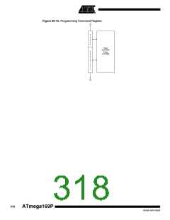
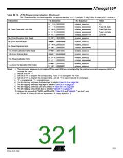
26.9.10 Programming Command Register
The Programming Command Register is a 15-bit register. This register is used to serially shift in
programming commands, and to serially shift out the result of the previous command, if any. The
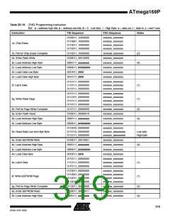
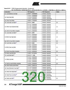
JTAG Programming Instruction Set is shown in Table 26-16. The state sequence when shifting
in the programming commands is illustrated in Figure 26-16.
317
8018A–AVR–03/06

 ATMEL [ ATMEL ]