ATmega169P
applied for a given address. The Program Memory Page is stored by loading the Write
Program Memory Page instruction with the 7 MSB of the address. If polling (RDY/BSY) is
not used, the user must wait at least tWD_FLASH before issuing the next page. (See Table
26-14.) Accessing the serial programming interface before the Flash write operation
completes can result in incorrect programming.
5. A: The EEPROM array is programmed one byte at a time by supplying the address and
data together with the appropriate Write instruction. An EEPROM memory location is first
automatically erased before new data is written. If polling (RDY/BSY) is not used, the
user must wait at least tWD_EEPROM before issuing the next byte (See Table 26-14). In a
chip erased device, no 0xFFs in the data file(s) need to be programmed.
B: The EEPROM array is programmed one page at a time. The Memory page is loaded
one byte at a time by supplying the 2 LSB of the address and data together with the Load
EEPROM Memory Page instruction. The EEPROM Memory Page is stored by loading
the Write EEPROM Memory Page Instruction with the 4 MSB of the address. When using
EEPROM page access only byte locations loaded with the Load EEPROM Memory Page
instruction is altered. The remaining locations remain unchanged. If polling (RDY/BSY) is
not used, the user must wait at least tWD_EEPROM before issuing the next page (See Table
26-14). In a chip erased device, no 0xFF in the data file(s) need to be programmed.
6. Any memory location can be verified by using the Read instruction which returns the con-
tent at the selected address at serial output MISO.
7. At the end of the programming session, RESET can be set high to commence normal
operation.
8. Power-off sequence (if needed):
Set RESET to “1”.
Turn VCC power off
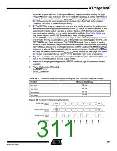
Table 26-14. Minimum Wait Delay Before Writing the Next Flash or EEPROM Location
Symbol
Minimum Wait Delay
4.5 ms
tWD_FUSE
tWD_FLASH
tWD_EEPROM
tWD_ERASE
4.5 ms
9.0 ms
9.0 ms
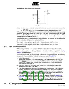
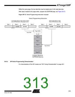
Figure 26-11. Serial Programming Waveforms
SERIAL DATA INPUT
(MOSI)
MSB
LSB
LSB
SERIAL DATA OUTPUT
(MISO)
MSB
SERIAL CLOCK INPUT
(SCK)
SAMPLE
311
8018A–AVR–03/06

 ATMEL [ ATMEL ]