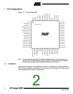
1. Pin Configurations
Figure 1-1. Pinout ATmega169P
LCDCAP
(RXD/PCINT0) PE0
(TXD/PCINT1) PE1
1
2
3
PA3 (COM3)
PA4 (SEG0)
PA5 (SEG1)
PA6 (SEG2)
48
47
46
INDEX CORNER
(XCK/AIN0/PCINT2) PE2
(AIN1/PCINT3) PE3
4
45
5
6
PA7 (SEG3)
PG2 (SEG4)
PC7 (SEG5)
PC6 (SEG6)
PC5 (SEG7)
44
43
(USCK/SCL/PCINT4) PE4
(DI/SDA/PCINT5) PE5
(DO/PCINT6) PE6
7
8
9
42
41
40
(CLKO/PCINT7) PE7
(SS/PCINT8) PB0 10
(SCK/PCINT9) PB1 11
(MOSI/PCINT10) PB2 12
(MISO/PCINT11) PB3 13
39 PC4 (SEG8)
PC3 (SEG9)
PC2 (SEG10)
PC1 (SEG11)
PC0 (SEG12)
38
37
36
(OC0A/PCINT12) PB4 14
(OC1A/PCINT13) PB5 15
(OC1B/PCINT14) PB6 16
35
34
33
PG1 (SEG13)
PG0 (SEG14)
Note:
The large center pad underneath the QFN/MLF packages is made of metal and internally con-
nected to GND. It should be soldered or glued to the board to ensure good mechanical stability. If
the center pad is left unconnected, the package might loosen from the board.
1.1
Disclaimer
Typical values contained in this datasheet are based on simulations and characterization of
other AVR microcontrollers manufactured on the same process technology. Min and Max values
will be available after the device is characterized.
2
ATmega169P
8018A–AVR–03/06

 ATMEL [ ATMEL ]