ATmega169P
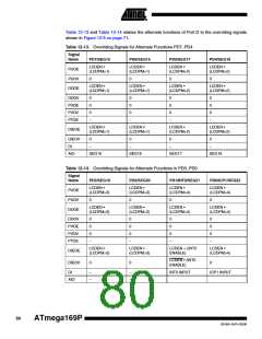
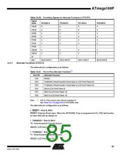
12.3.5
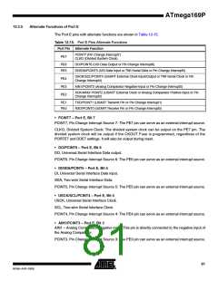
Alternate Functions of Port E
The Port E pins with alternate functions are shown in Table 12-15.
Table 12-15. Port E Pins Alternate Functions
Port Pin
Alternate Function
PCINT7 (Pin Change Interrupt7)
CLKO (Divided System Clock)
PE7
PE6
PE5
DO/PCINT6 (USI Data Output or Pin Change Interrupt6)
DI/SDA/PCINT5 (USI Data Input or TWI Serial DAta or Pin Change Interrupt5)
USCK/SCL/PCINT4 (USART External Clock Input/Output or TWI Serial Clock or Pin
Change Interrupt4)
PE4
PE3
PE2
AIN1/PCINT3 (Analog Comparator Negative Input or Pin Change Interrupt3)
XCK/AIN0/ PCINT2 (USART External Clock or Analog Comparator Positive Input or Pin
Change Interrupt2)
PE1
PE0
TXD/PCINT1 (USART Transmit Pin or Pin Change Interrupt1)
RXD/PCINT0 (USART Receive Pin or Pin Change Interrupt0)
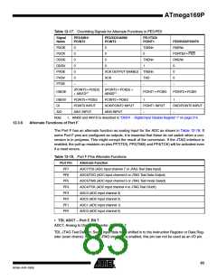
• PCINT7 – Port E, Bit 7
PCINT7, Pin Change Interrupt Source 7: The PE7 pin can serve as an external interrupt source.
CLKO, Divided System Clock: The divided system clock can be output on the PE7 pin. The
divided system clock will be output if the CKOUT Fuse is programmed, regardless of the
PORTE7 and DDE7 settings. It will also be output during reset.
• DO/PCINT6 – Port E, Bit 6
DO, Universal Serial Interface Data output.
PCINT6, Pin Change Interrupt Source 6: The PE6 pin can serve as an external interrupt source.
• DI/SDA/PCINT5 – Port E, Bit 5
DI, Universal Serial Interface Data input.
SDA, Two-wire Serial Interface Data:
PCINT5, Pin Change Interrupt Source 5: The PE5 pin can serve as an external interrupt source.
• USCK/SCL/PCINT4 – Port E, Bit 4
USCK, Universal Serial Interface Clock.
SCL, Two-wire Serial Interface Clock.
PCINT4, Pin Change Interrupt Source 4: The PE4 pin can serve as an external interrupt source.
• AIN1/PCINT3 – Port E, Bit 3
AIN1 – Analog Comparator Negative input. This pin is directly connected to the negative input of
the Analog Comparator.
PCINT3, Pin Change Interrupt Source 3: The PE3 pin can serve as an external interrupt source.
81
8018A–AVR–03/06

 ATMEL [ ATMEL ]