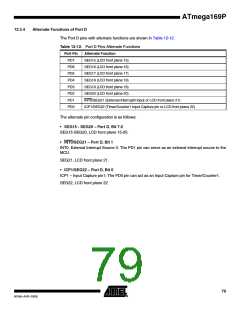
low. When the SPI is enabled as a Master, the data direction of this pin is controlled by DDB0.
When the pin is forced to be an input, the pull-up can still be controlled by the PORTB0 bit
PCINT8, Pin Change Interrupt Source 8: The PB0 pin can serve as an external interrupt source.
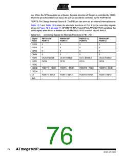
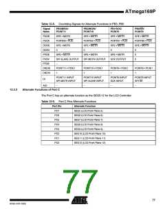
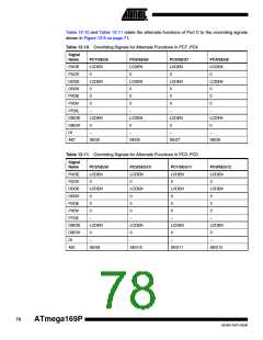
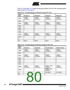
Table 12-7 and Table 12-8 relate the alternate functions of Port B to the overriding signals
shown in Figure 12-5 on page 71. SPI MSTR INPUT and SPI SLAVE OUTPUT constitute the
MISO signal, while MOSI is divided into SPI MSTR OUTPUT and SPI SLAVE INPUT.
Table 12-7. Overriding Signals for Alternate Functions in PB7..PB4
Signal
Name
PB7/OC2A/
PCINT15
PB6/OC1B/
PCINT14
PB5/OC1A/
PCINT13
PB4/OC0A/
PCINT12
PUOE
PUOV
DDOE
DDOV
PVOE
PVOV
PTOE
DIEOE
DIEOV
DI
0
0
0
0
0
0
0
0
0
0
0
0
0
0
0
0
OC2A ENABLE
OC1B ENABLE
OC1A ENABLE
OC0A ENABLE
OC2A
OC1B
OC1A
OC0A
–
–
–
–
PCINT15 • PCIE1
PCINT14 • PCIE1
PCINT13 • PCIE1
PCINT12 • PCIE1
1
1
1
1
PCINT15 INPUT
–
PCINT14 INPUT
–
PCINT13 INPUT
–
PCINT12 INPUT
–
AIO
76
ATmega169P
8018A–AVR–03/06

 ATMEL [ ATMEL ]