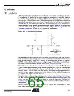
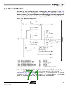
ATmega169P
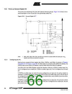
12.2.2
12.2.3
Toggling the Pin
Writing a logic one to PINxn toggles the value of PORTxn, independent on the value of DDRxn.
Note that the SBI instruction can be used to toggle one single bit in a port.
Switching Between Input and Output
When switching between tri-state ({DDxn, PORTxn} = 0b00) and output high ({DDxn, PORTxn}
= 0b11), an intermediate state with either pull-up enabled {DDxn, PORTxn} = 0b01) or output
low ({DDxn, PORTxn} = 0b10) must occur. Normally, the pull-up enabled state is fully accept-
able, as a high-impedant environment will not notice the difference between a strong high driver
and a pull-up. If this is not the case, the PUD bit in the MCUCR Register can be set to disable all
pull-ups in all ports.
Switching between input with pull-up and output low generates the same problem. The user
must use either the tri-state ({DDxn, PORTxn} = 0b00) or the output high state ({DDxn, PORTxn}
= 0b11) as an intermediate step.
Table 12-1 on page 67 summarizes the control signals for the pin value.
Table 12-1. Port Pin Configurations
PUD
DDxn
PORTxn
(in MCUCR)
I/O
Pull-up
No
Comment
0
0
1
1
0
1
X
0
Input
Tri-state (Hi-Z)
0
Input
Yes
No
Pxn will source current if ext. pulled low.
Tri-state (Hi-Z)
0
1
Input
1
X
X
Output
Output
No
Output Low (Sink)
Output High (Source)
1
No
12.2.4
Reading the Pin Value
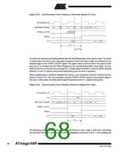
Independent of the setting of Data Direction bit DDxn, the port pin can be read through the
PINxn Register bit. As shown in Figure 12-2, the PINxn Register bit and the preceding latch con-
stitute a synchronizer. This is needed to avoid metastability if the physical pin changes value
near the edge of the internal clock, but it also introduces a delay. Figure 12-3 shows a timing dia-
gram of the synchronization when reading an externally applied pin value. The maximum and
minimum propagation delays are denoted tpd,max and tpd,min respectively.
67
8018A–AVR–03/06

 ATMEL [ ATMEL ]