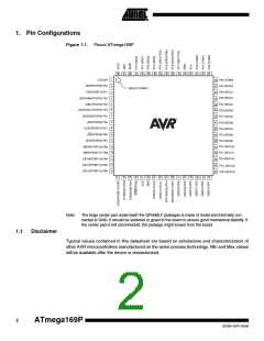
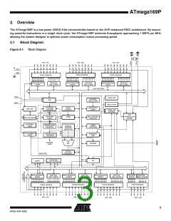
2.2.7
Port E (PE7:PE0)
Port E is an 8-bit bi-directional I/O port with internal pull-up resistors (selected for each bit). The
Port E output buffers have symmetrical drive characteristics with both high sink and source
capability. As inputs, Port E pins that are externally pulled low will source current if the pull-up
resistors are activated. The Port E pins are tri-stated when a reset condition becomes active,
even if the clock is not running.
Port E also serves the functions of various special features of the ATmega169P as listed on
”Alternate Functions of Port E” on page 81.
2.2.8
Port F (PF7:PF0)
Port F serves as the analog inputs to the A/D Converter.
Port F also serves as an 8-bit bi-directional I/O port, if the A/D Converter is not used. Port pins
can provide internal pull-up resistors (selected for each bit). The Port F output buffers have sym-
metrical drive characteristics with both high sink and source capability. As inputs, Port F pins
that are externally pulled low will source current if the pull-up resistors are activated. The Port F
pins are tri-stated when a reset condition becomes active, even if the clock is not running. If the
JTAG interface is enabled, the pull-up resistors on pins PF7(TDI), PF5(TMS), and PF4(TCK) will
be activated even if a reset occurs.
Port F also serves the functions of the JTAG interface, see ”Alternate Functions of Port F” on
page 83
2.2.9
Port G (PG5:PG0)
Port G is a 6-bit bi-directional I/O port with internal pull-up resistors (selected for each bit). The
Port G output buffers have symmetrical drive characteristics with both high sink and source
capability. As inputs, Port G pins that are externally pulled low will source current if the pull-up
resistors are activated. The Port G pins are tri-stated when a reset condition becomes active,
even if the clock is not running.
Port G also serves the functions of various special features of the ATmega169P as listed on
page 85.
2.2.10
RESET
Reset input. A low level on this pin for longer than the minimum pulse length will generate a
reset, even if the clock is not running. The minimum pulse length is given in Table 9-1 on page
47. Shorter pulses are not guaranteed to generate a reset.
2.2.11
2.2.12
2.2.13
XTAL1
XTAL2
AVCC
Input to the inverting Oscillator amplifier and input to the internal clock operating circuit.
Output from the inverting Oscillator amplifier.
AVCC is the supply voltage pin for Port F and the A/D Converter. It should be externally con-
nected to VCC, even if the ADC is not used. If the ADC is used, it should be connected to VCC
through a low-pass filter.
6
ATmega169P
8018A–AVR–03/06

 ATMEL [ ATMEL ]