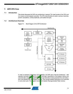
ATmega640/1280/1281/2560/2561
resistors are activated. The Port H pins are tri-stated when a reset condition becomes active,
even if the clock is not running.
Port H also serves the functions of various special features of the ATmega640/1280/2560 as
listed on page 92.
3.3.11
Port J (PJ7..PJ0)
Port J is a 8-bit bi-directional I/O port with internal pull-up resistors (selected for each bit). The
Port J output buffers have symmetrical drive characteristics with both high sink and source capa-
bility. As inputs, Port J pins that are externally pulled low will source current if the pull-up
resistors are activated. The Port J pins are tri-stated when a reset condition becomes active,
even if the clock is not running.
Port J also serves the functions of various special features of the ATmega640/1280/2560 as
listed on page 95.
3.3.12
Port K (PK7..PK0)
Port K serves as analog inputs to the A/D Converter.
Port K is a 8-bit bi-directional I/O port with internal pull-up resistors (selected for each bit). The
Port K output buffers have symmetrical drive characteristics with both high sink and source
capability. As inputs, Port K pins that are externally pulled low will source current if the pull-up
resistors are activated. The Port K pins are tri-stated when a reset condition becomes active,
even if the clock is not running.
Port K also serves the functions of various special features of the ATmega640/1280/2560 as
listed on page 96.
3.3.13
Port L (PL7..PL0)
Port L is a 8-bit bi-directional I/O port with internal pull-up resistors (selected for each bit). The
Port L output buffers have symmetrical drive characteristics with both high sink and source
capability. As inputs, Port L pins that are externally pulled low will source current if the pull-up
resistors are activated. The Port L pins are tri-stated when a reset condition becomes active,
even if the clock is not running.
Port L also serves the functions of various special features of the ATmega640/1280/2560 as
listed on page 98.
3.3.14
RESET
Reset input. A low level on this pin for longer than the minimum pulse length will generate a
reset, even if the clock is not running. The minimum pulse length is given in “System and Reset
Characteristics” on page 375. Shorter pulses are not guaranteed to generate a reset.
3.3.15
3.3.16
XTAL1
XTAL2
Input to the inverting Oscillator amplifier and input to the internal clock operating circuit.
Output from the inverting Oscillator amplifier.
9
2549L–AVR–08/07

 ATMEL [ ATMEL ]