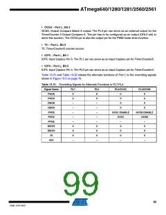
Table 13-32. Overriding Signals for Alternate Functions in PL3:PL0
Signal Name
PUOE
PUOV
DDOE
DDOV
PVOE
PVOV
PTOE
DIEOE
DIEOV
DI
PL3/OC5A
PL2/T5
PL1/ICP5
PL0/ICP4
0
0
0
0
0
0
0
0
0
0
0
0
0
0
0
0
OC5A ENABLE
0
0
0
OC5A
0
0
0
–
0
0
0
–
–
–
–
0
0
0
0
T5 INPUT
–
0
0
ICP5 INPUT
ICP4 INPUT
AIO
–
–
13.4 Register Description for I/O-Ports
13.4.1
MCUCR – MCU Control Register
Bit
7
6
–
5
–
4
3
–
2
1
0
0x35 (0x55)
Read/Write
Initial Value
JTD
R/W
0
PUD
R/W
0
–
R
0
IVSEL
R/W
0
IVCE
R/W
0
MCUCR
R
0
R
0
R
0
• Bit 4 – PUD: Pull-up Disable
When this bit is written to one, the I/O ports pull-up resistors are disabled even if the DDxn and
PORTxn Registers are configured to enable the pull-up resistor ({DDxn, PORTxn} = 0b01). See
“Configuring the Pin” on page 71 for more details about this feature.
13.4.2
13.4.3
13.4.4
PORTA – Port A Data Register
Bit
7
6
PORTA6
R/W
0
5
PORTA5
R/W
0
4
PORTA4
R/W
0
3
PORTA3
R/W
0
2
PORTA2
R/W
0
1
PORTA1
R/W
0
0
PORTA0
R/W
0
PORTA7
R/W
0
0x02 (0x22)
Read/Write
Initial Value
PORTA
DDRA
PINA
DDRA – Port A Data Direction Register
Bit
7
DDA7
R/W
0
6
DDA6
R/W
0
5
DDA5
R/W
0
4
DDA4
R/W
0
3
DDA3
R/W
0
2
DDA2
R/W
0
1
DDA1
R/W
0
0
DDA0
R/W
0
0x01 (0x21)
Read/Write
Initial Value
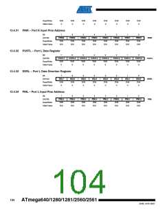
PINA – Port A Input Pins Address
Bit
7
6
5
4
3
2
1
0
0x00 (0x20)
Read/Write
Initial Value
PINA7
R/W
N/A
PINA6
R/W
N/A
PINA5
R/W
N/A
PINA4
R/W
N/A
PINA3
R/W
N/A
PINA2
R/W
N/A
PINA1
R/W
N/A
PINA0
R/W
N/A
100
ATmega640/1280/1281/2560/2561
2549L–AVR–08/07

 ATMEL [ ATMEL ]