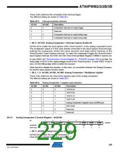
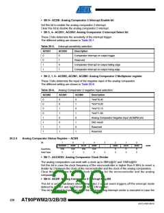
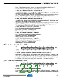
AT90PWM2/3/2B/3B
21. Analog to Digital Converter - ADC
21.1 Features
• 10-bit Resolution
• 0.5 LSB Integral Non-linearity
•
2 LSB Absolute Accuracy
• 8- 320 µs Conversion Time
• Up to 125 kSPS at Maximum Resolution
• 11 Multiplexed Single Ended Input Channels
• Two Differential input channels with accurate programmable gain 5, 10, 20 and 40
• Optional Left Adjustment for ADC Result Readout
• 0 - VCC ADC Input Voltage Range
• Selectable 2.56 V ADC Reference Voltage
• Free Running or Single Conversion Mode
• ADC Start Conversion by Auto Triggering on Interrupt Sources
• Interrupt on ADC Conversion Complete
• Sleep Mode Noise Canceler
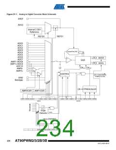
The AT90PWM2/2B/3/3B features a 10-bit successive approximation ADC. The ADC is con-
nected to an 15-channel Analog Multiplexer which allows eleven single-ended input. The single-
ended voltage inputs refer to 0V (GND).
The device also supports 2 differential voltage input combinations which are equipped with a
programmable gain stage, providing amplification steps of 14dB (5x), 20 dB (10x), 26 dB (20x),
or 32dB (40x) on the differential input voltage before the A/D conversion. On the amplified chan-
nels, 8-bit resolution can be expected.
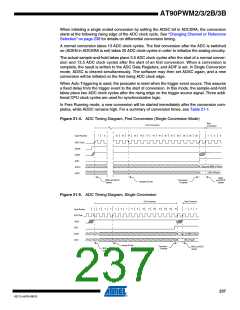
The ADC contains a Sample and Hold circuit which ensures that the input voltage to the ADC is
held at a constant level during conversion. A block diagram of the ADC is shown in Figure 21-1.
The ADC has a separate analog supply voltage pin, AVCC. AVCC must not differ more than
0.3V from VCC. See the paragraph “ADC Noise Canceler” on page 240 on how to connect this
pin.
Internal reference voltages of nominally 2.56V or AVCC are provided On-chip. The voltage refer-
ence may be externally decoupled at the AREF pin by a capacitor for better noise performance.
233
4317J–AVR–08/10

 ATMEL [ ATMEL ]