These 2 bits determine the sensitivity of the interrupt trigger.
The different setting are shown in Table 20-1.
Table 20-1. Interrupt sensitivity selection
AC0IS1
AC0IS0
Description
0
0
1
1
0
1
0
1
Comparator Interrupt on output toggle
Reserved
Comparator interrupt on output falling edge
Comparator interrupt on output rising edge
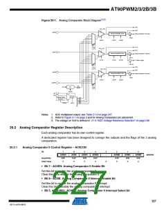
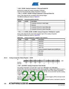
• Bit 2, 1, 0– AC0M2, AC0M1, AC0M0: Analog Comparator 0 Multiplexer register
These 3 bits determine the input of the negative input of the analog comparator.
The different setting are shown in Table 20-2.
Table 20-2. Analog Comparator 0 negative input selection
AC0M2
AC0M1
AC0M0
Description
0
0
0
0
1
1
1
1
0
0
1
1
0
0
1
1
0
1
0
1
0
1
0
1
“Vref”/6.40
“Vref”/3.20
“Vref”/2.13
“Vref”/1.60
Analog Comparator Negative Input (ACMPM pin)
DAC result
Reserved
Reserved
20.2.2
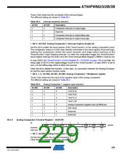
Analog Comparator 1Control Register – AC1CON
Bit
7
AC1EN
R/W
0
6
AC1IE
R/W
0
5
AC1IS1
R/W
0
4
AC1IS0
R/W
0
3
AC1ICE
R/W
0
2
AC1M2
R/W
0
1
AC1M1
R/W
0
0
AC1M0
R/W
0
AC1CON
Read/Write
Initial Value
• Bit 7– AC1EN: Analog Comparator 1 Enable Bit
Set this bit to enable the analog comparator 1.
Clear this bit to disable the analog comparator 1.
• Bit 6– AC1IE: Analog Comparator 1 Interrupt Enable bit
Set this bit to enable the analog comparator 1 interrupt.
Clear this bit to disable the analog comparator 1 interrupt.
• Bit 5, 4– AC1IS1, AC1IS0: Analog Comparator 1 Interrupt Select bit
228
AT90PWM2/3/2B/3B
4317J–AVR–08/10

 ATMEL [ ATMEL ]