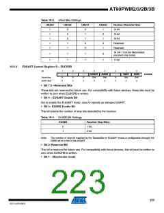
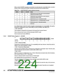
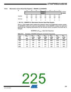
AT90PWM2/3/2B/3B
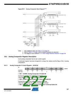
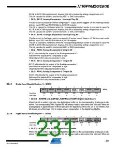
Figure 20-1. Analog Comparator Block Diagram(1)(2)
AC0O
AC0IF
CLKI/O (/2)
ACMP0
+
-
Interrupt Sensitivity Control
Analog Comparator 0 Interrupt
AC0IE
AC0EN
AC0IS1
AC0IS0
AC1O
AC1IF
AC0M
(/2)
CLKI/O
2
1 0
ACMP1
+
-
Interrupt Sensitivity Control
Analog Comparator 1 Interrupt
AC1IE
AC1EN
AC1IS1
AC1IS0
T1 Capture Trigger
AC1ICE
AC2O
AC2IF
AC1M
I/O (/2)
CLK
2
1 0
ACMP2
+
-
Interrupt Sensitivity Control
Analog Comparator 2 Interrupt
AC0IE
AC2EN
AC2IS1
AC2IS0
ACMPM
DAC
Vref
DAC
Result
AC2M
2
1 0
DACEN
Aref
AVcc
Internal 2.56V
Reference
/1.60
/2.13
/3.20
/6.40
REFS0
REFS1
Notes: 1. ADC multiplexer output: see Table 21-4 on page 247.
2. Refer to Figure 3-1 on page 3 and for Analog Comparator pin placement.
3. The voltage on Vref is defined in 21-3 “ADC Voltage Reference Selection” on page 246
20.2 Analog Comparator Register Description
Each analog comparator has its own control register.
A dedicated register has been designed to consign the outputs and the flags of the 3 analog
comparators.
20.2.1
Analog Comparator 0 Control Register – AC0CON
Bit
7
6
5
4
AC0IS0
R/W
0
3
-
2
AC0M2
R/W
0
1
AC0M1
R/W
0
0
AC0M0
R/W
0
AC0EN
AC0IE
AC0IS1
AC0CON
Read/Write
Initial Value
R/W
0
R/W
0
R/W
0
-
0
• Bit 7– AC0EN: Analog Comparator 0 Enable Bit
Set this bit to enable the analog comparator 0.
Clear this bit to disable the analog comparator 0.
• Bit 6– AC0IE: Analog Comparator 0 Interrupt Enable bit
Set this bit to enable the analog comparator 0 interrupt.
Clear this bit to disable the analog comparator 0 interrupt.
• Bit 5, 4– AC0IS1, AC0IS0: Analog Comparator 0 Interrupt Select bit
227
4317J–AVR–08/10

 ATMEL [ ATMEL ]