AT89S52
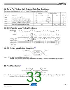
34. Serial Port Timing: Shift Register Mode Test Conditions
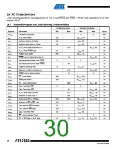
The values in this table are valid for VCC = 4.0V to 5.5V and Load Capacitance = 80 pF.
12 MHz Osc
Variable Oscillator
Symbol
tXLXL
Parameter
Min
Max
Min
12 tCLCL
10 tCLCL-133
2 tCLCL-80
0
Max
Units
μs
Serial Port Clock Cycle Time
1.0
700
50
0
tQVXH
tXHQX
tXHDX
tXHDV
Output Data Setup to Clock Rising Edge
Output Data Hold After Clock Rising Edge
Input Data Hold After Clock Rising Edge
Clock Rising Edge to Input Data Valid
ns
ns
ns
700
10 tCLCL-133
ns
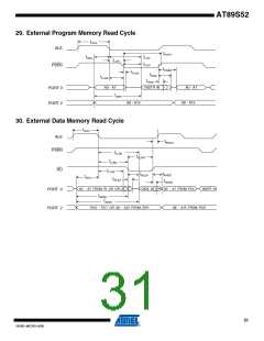
35. Shift Register Mode Timing Waveforms
INSTRUCTION
ALE
0
1
2
3
4
5
6
7
8
tXLXL
CLOCK
tQVXH
tXHQX
1
WRITE TO SBUF
0
2
3
4
5
6
7
tXHDX
SET TI
tXHDV
OUTPUT DATA
CLEAR RI
VALID
VALID
VALID
VALID
VALID
VALID
VALID
VALID
SET RI
INPUT DATA
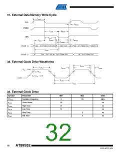
36. AC Testing Input/Output Waveforms(1)
VCC - 0.5V
0.2 VCC + 0.9V
TEST POINTS
0.2 VCC - 0.1V
0.45V
Note:
1. AC Inputs during testing are driven at VCC - 0.5V
for a logic 1 and 0.45V for a logic 0. Timing measurements are made at VIH min. for a logic 1 and VIL max. for a logic 0.
37. Float Waveforms(1)
+ 0.1V
- 0.1V
- 0.1V
+ 0.1V
VOL
VLOAD
Timing Reference
Points
VLOAD
VLOAD
VOL
Note:
1. For timing purposes, a port pin is no longer floating when a 100 mV change from load voltage occurs. A port pin begins to
float when a 100 mV change from the loaded VOH/VOL level occurs.
33
1919D–MICRO–6/08

 ATMEL [ ATMEL ]