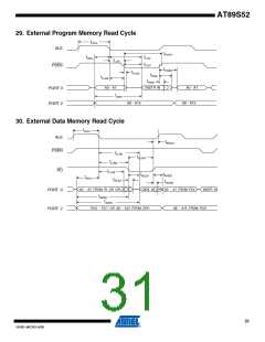
AT89S52
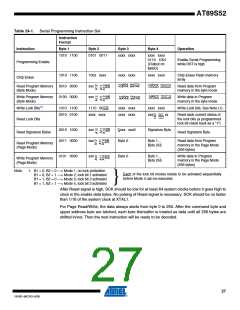
Table 24-1. Serial Programming Instruction Set
Instruction
Format
Instruction
Byte 1
Byte 2
Byte 3
Byte 4
Operation
1010 1100
0101 0011
xxxx xxxx
xxxx xxxx
0110 1001
(Output on
MISO)
Enable Serial Programming
while RST is high
Programming Enable
1010 1100
0010 0000
0100 0000
100x xxxx
xxx
xxxx xxxx
xxxx xxxx
Chip Erase Flash memory
array
Chip Erase
Read Program Memory
(Byte Mode)
Read data from Program
memory in the byte mode
Write Program Memory
(Byte Mode)
xxx
Write data to Program
memory in the byte mode
Write Lock Bits(1)
1010 1100
0010 0100
1110 00
xxxx xxxx
xxxx xxxx
xxxx xxxx
Write Lock bits. See Note (1).
xxxx xxxx
xxx
xx
Read back current status of
the lock bits (a programmed
lock bit reads back as a “1”)
Read Lock Bits
0010 1000
0011 0000
xxx
xxx
xxx xxx0
Byte 0
Signature Byte
Read Signature Bytes
Read Signature Byte
Byte 1...
Byte 255
Read data from Program
memory in the Page Mode
(256 bytes)
Read Program Memory
(Page Mode)
0101 0000
xxx
Byte 0
Byte 1...
Byte 255
Write data to Program
memory in the Page Mode
(256 bytes)
Write Program Memory
(Page Mode)
Note:
1. B1 = 0, B2 = 0 ---> Mode 1, no lock protection
B1 = 0, B2 = 1 ---> Mode 2, lock bit 1 activated
B1 = 1, B2 = 0 ---> Mode 3, lock bit 2 activated
B1 = 1, B2 = 1 ---> Mode 4, lock bit 3 activated
Each of the lock bit modes needs to be activated sequentially
before Mode 4 can be executed.
}
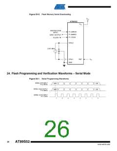
After Reset signal is high, SCK should be low for at least 64 system clocks before it goes high to
clock in the enable data bytes. No pulsing of Reset signal is necessary. SCK should be no faster
than 1/16 of the system clock at XTAL1.
For Page Read/Write, the data always starts from byte 0 to 255. After the command byte and
upper address byte are latched, each byte thereafter is treated as data until all 256 bytes are
shifted in/out. Then the next instruction will be ready to be decoded.
27
1919D–MICRO–6/08

 ATMEL [ ATMEL ]