6. Memory Organization
MCS-51 devices have a separate address space for Program and Data Memory. Up to 64K
bytes each of external Program and Data Memory can be addressed.
6.1
6.2
Program Memory
If the EA pin is connected to GND, all program fetches are directed to external memory.
On the AT89S52, if EA is connected to VCC, program fetches to addresses 0000H through
1FFFH are directed to internal memory and fetches to addresses 2000H through FFFFH are to
external memory.
Data Memory
The AT89S52 implements 256 bytes of on-chip RAM. The upper 128 bytes occupy a parallel
address space to the Special Function Registers. This means that the upper 128 bytes have the
same addresses as the SFR space but are physically separate from SFR space.
When an instruction accesses an internal location above address 7FH, the address mode used
in the instruction specifies whether the CPU accesses the upper 128 bytes of RAM or the SFR
space. Instructions which use direct addressing access the SFR space.
For example, the following direct addressing instruction accesses the SFR at location 0A0H
(which is P2).
MOV 0A0H, #data
Instructions that use indirect addressing access the upper 128 bytes of RAM. For example, the
following indirect addressing instruction, where R0 contains 0A0H, accesses the data byte at
address 0A0H, rather than P2 (whose address is 0A0H).
MOV @R0, #data
Note that stack operations are examples of indirect addressing, so the upper 128 bytes of data
RAM are available as stack space.
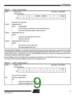
7. Watchdog Timer (One-time Enabled with Reset-out)
The WDT is intended as a recovery method in situations where the CPU may be subjected to
software upsets. The WDT consists of a 14-bit counter and the Watchdog Timer Reset
(WDTRST) SFR. The WDT is defaulted to disable from exiting reset. To enable the WDT, a user
must write 01EH and 0E1H in sequence to the WDTRST register (SFR location 0A6H). When
the WDT is enabled, it will increment every machine cycle while the oscillator is running. The
WDT timeout period is dependent on the external clock frequency. There is no way to disable
the WDT except through reset (either hardware reset or WDT overflow reset). When WDT over-
flows, it will drive an output RESET HIGH pulse at the RST pin.
7.1
Using the WDT
To enable the WDT, a user must write 01EH and 0E1H in sequence to the WDTRST register
(SFR location 0A6H). When the WDT is enabled, the user needs to service it by writing 01EH
and 0E1H to WDTRST to avoid a WDT overflow. The 14-bit counter overflows when it reaches
16383 (3FFFH), and this will reset the device. When the WDT is enabled, it will increment every
machine cycle while the oscillator is running. This means the user must reset the WDT at least
every 16383 machine cycles. To reset the WDT the user must write 01EH and 0E1H to
WDTRST. WDTRST is a write-only register. The WDT counter cannot be read or written. When
10
AT89S52
1919C–MICRO–3/05

 ATMEL [ ATMEL ]