7.6
Sector Erase
The Sector Erase command can be used to individually erase any sector in the main memory.
There are 16 sectors and only one sector can be erased at one time. To perform sector 0a or
sector 0b erase for the standard DataFlash page size (528 bytes), an opcode of 7CH must be
loaded into the device, followed by three address bytes comprised of 2 don’t care bits, 9 page
address bits (PA11 - PA3) and 13 don’t care bits. To perform a sector 1-15 erase, the opcode
7CH must be loaded into the device, followed by three address bytes comprised of 2 don’t care
bits, 4 page address bits (PA11 - PA8) and 18 don’t care bits. To perform sector 0a or sector 0b
erase for the binary page size (512 bytes), an opcode of 7CH must be loaded into the device,
followed by three address bytes comprised of 3 don’t care bit and 9 page address bits (A20 -
A12) and 12 don’t care bits. To perform a sector 1-15 erase, the opcode 7CH must be loaded
into the device, followed by three address bytes comprised of 3 don’t care bit and 4 page
address bits (A20 - A17) and 17 don’t care bits. The page address bits are used to specify any
valid address location within the sector which is to be erased. When a low-to-high transition
occurs on the CS pin, the part will erase the selected sector. The erase operation is internally
self-timed and should take place in a maximum time of tSE. During this time, the status register
and the RDY/BUSY pin will indicate that the part is busy.
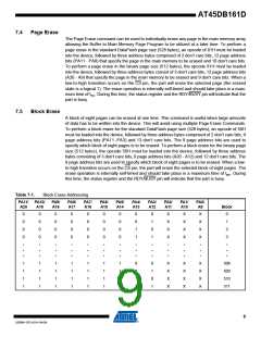
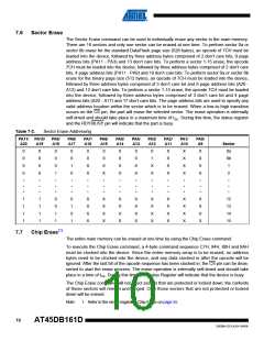
Table 7-2.
Sector Erase Addressing
PA11/ PA10/
PA9/
A18
PA8/
A17
PA7/
A16
PA6/
A15
PA5/
A14
PA4/
A13
PA3/
A12
PA2/
A11
PA1/
A10
PA0/
A9
A20
A19
Sector
0
0
0
0
0
1
0
0
1
0
0
0
0
0
0
0
0
0
0
1
X
X
X
X
X
X
X
X
X
X
X
X
0a
0b
1
0
0
0
0
X
X
X
X
X
X
X
X
X
X
0
0
2
•
•
•
•
•
•
•
•
•
•
•
•
•
•
•
•
•
•
•
•
•
•
•
•
•
•
•
•
•
•
•
•
•
•
•
•
•
•
•
1
1
1
1
1
1
1
1
0
0
1
1
0
1
0
1
X
X
X
X
X
X
X
X
X
X
X
X
X
X
X
X
X
X
X
X
X
X
X
X
X
X
X
X
X
X
X
X
12
13
14
15
7.7
Chip Erase(1)
The entire main memory can be erased at one time by using the Chip Erase command.
To execute the Chip Erase command, a 4-byte command sequence C7H, 94H, 80H and 9AH
must be clocked into the device. Since the entire memory array is to be erased, no address
bytes need to be clocked into the device, and any data clocked in after the opcode will be
ignored. After the last bit of the opcode sequence has been clocked in, the CS pin can be deas-
serted to start the erase process. The erase operation is internally self-timed and should take
place in a time of tCE. During this time, the Status Register will indicate that the device is busy.
The Chip Erase command will not affect sectors that are protected or locked down; the contents
of those sectors will remain unchanged. Only those sectors that are not protected or locked
down will be erased.
Note:
1. Refer to the errata regarding Chip Erase on page 55.
10
AT45DB161D
3500M–DFLASH–04/09

 ATMEL [ ATMEL ]