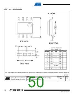
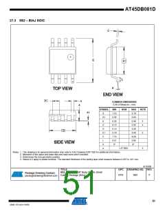
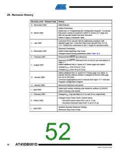
28. Revision History
Revision Level – Release Date History
A – November 2005
B – March 2006
Initial Release
Added Preliminary.
Added text, in “Programming the Configuration Register”, to indicate
that power cycling is required to switch to “power of 2” page size
after the opcode enable has been executed.
Added “Legacy Commands” table.
Corrected PA3 in opcode 50h for addressing sequence with
standard page size. Corrected Chip Erase opcode from 7CH to
C7H. Clarified the commands B and C usage for operation mode.
C – July 2006
Removed Preliminary.
D – November 2006
E – February 2007
Added errata regarding Chip Erase.
Changed various timing parameters under Table 18-4.
Removed RDY/BUSY pin references.
Removed SER/BYTE statement from SI and SO pin descriptions in
Table 2-1.
Added additional text to “power of 2” binary page size option.
F – August 2007
G – January 2008
Changed tVSCL from 50 µs to 70 µs.
Changed tRDPD from 30 µs to 35 µs.
Added additional text, in “power of 2” binary page size option, to
indicate that the address format is changed for devices with page
size set to 256 bytes.
Corrected typographical error to indicate that Figure 13-1 indicates
Program Configuration Register.
H – January 2008
I – April 2008
Removed DataFlash card pinout.
Added part number ordering code details for suffixes SL954/955
Added ordering code details.
J – February 2009
Changed tDIS (Typ and Max) to 27 ns and 35 ns, respectively.
Changed Deep Power-Down Current values
- Increased typical value from 5 µA to 15 µA.
- Increased maximum value from 15 µA to 25 µA.
K – March 2009
L - April 2009
Updated Absolute Maximum Ratings
Removed Chip Erase Errata
52
AT45DB081D
3596L–DFLASH–04/09

 ATMEL [ ATMEL ]