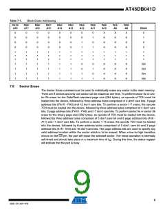
Table 7-2.
Sector Erase Addressing
PA10/
A18
PA9/
A17
PA8/
A16
PA7/
A15
PA6/
A14
PA5/
A13
PA4/
A12
PA3/
A11
PA2/
A10
PA1/
A9
PA0/
A8
Sector
0
0
0
0
0
0
0
1
0
0
1
0
0
0
0
0
0
0
0
0
0
1
X
X
X
X
X
X
X
X
X
X
X
X
0a
0b
1
X
X
X
X
X
X
X
X
X
X
2
•
•
•
•
•
•
•
•
•
•
•
•
•
•
•
•
•
•
•
•
•
•
•
•
•
•
•
•
•
•
•
•
•
•
•
•
1
1
1
1
0
0
1
1
0
1
0
1
X
X
X
X
X
X
X
X
X
X
X
X
X
X
X
X
X
X
X
X
X
X
X
X
X
X
X
X
X
X
X
X
4
5
6
7
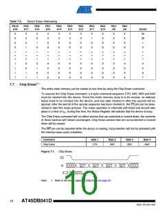
7.7
Chip Erase(1)
The entire main memory can be erased at one time by using the Chip Erase command.
To execute the Chip Erase command, a 4-byte command sequence C7H, 94H, 80H and 9AH
must be clocked into the device. Since the entire memory array is to be erased, no address
bytes need to be clocked into the device, and any data clocked in after the opcode will be
ignored. After the last bit of the opcode sequence has been clocked in, the CS pin can be deas-
serted to start the erase process. The erase operation is internally self-timed and should take
place in a time of tCE. During this time, the Status Register will indicate that the device is busy.
The Chip Erase command will not affect sectors that are protected or locked down; the contents
of those sectors will remain unchanged. Only those sectors that are not protected or locked
down will be erased.
The WP pin can be asserted while the device is erasing, but protection will not be activated until
the internal erase cycle completes.
Command
Byte 1
Byte 2
Byte 3
Byte 4
Chip Erase
C7H
94H
80H
9AH
Figure 7-1. Chip Erase
CS
Opcode
Byte 1
Opcode
Byte 2
Opcode
Byte 3
Opcode
Byte 4
SI
Each transition
represents 8 bits
Note:
1. Refer to the errata regarding Chip Erase on page 52.
10
AT45DB041D
3595L–DFLASH–4/08

 ATMEL [ ATMEL ]