AT45DB081D
The WP pin can be asserted while the device is erasing, but protection will not be activated until
the internal erase cycle completes.
Command
Byte 1
Byte 2
Byte 3
Byte 4
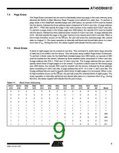
Chip Erase
C7H
94H
80H
9AH
Figure 7-1. Chip Erase
CS
Opcode
Byte 1
Opcode
Byte 2
Opcode
Byte 3
Opcode
Byte 4
SI
Each transition
represents 8 bits
Note:
Refer to errata regarding Chip Erase on page 52.
7.8
Main Memory Page Program Through Buffer
This operation is a combination of the Buffer Write and Buffer to Main Memory Page Program
with Built-in Erase operations. Data is first clocked into buffer 1 or buffer 2 from the input pin (SI)
and then programmed into a specified page in the main memory. To perform a main memory
page program through buffer for the DataFlash standard page size (264 bytes), a 1-byte opcode,
82H for buffer 1 or 85H for buffer 2, must first be clocked into the device, followed by three
address bytes. The address bytes are comprised of 3 don’t care bits, 12 page address bits,
(PA11 - PA0) that select the page in the main memory where data is to be written, and 9 buffer
address bits (BFA8 - BFA0) that select the first byte in the buffer to be written. To perform a
main memory page program through buffer for the binary page size (256 bytes), the opcode 82H
for buffer 1 or 85H for buffer 2, must be clocked into the device followed by three address bytes
consisting of 4 don’t care bits, 12 page address bits (A19 - A8) that specify the page in the main
memory to be written, and 8 buffer address bits (BFA7 - BFA0) that selects the first byte in the
buffer to be written. After all address bytes are clocked in, the part will take data from the input
pins and store it in the specified data buffer. If the end of the buffer is reached, the device will
wrap around back to the beginning of the buffer. When there is a low-to-high transition on the CS
pin, the part will first erase the selected page in main memory to all 1s and then program the
data stored in the buffer into that memory page. Both the erase and the programming of the
page are internally self-timed and should take place in a maximum time of tEP. During this time,
the status register will indicate that the part is busy.
8. Sector Protection
Two protection methods, hardware and software controlled, are provided for protection against
inadvertent or erroneous program and erase cycles. The software controlled method relies on
the use of software commands to enable and disable sector protection while the hardware con-
trolled method employs the use of the Write Protect (WP) pin. The selection of which sectors
that are to be protected or unprotected against program and erase operations is specified in the
nonvolatile Sector Protection Register. The status of whether or not sector protection has been
enabled or disabled by either the software or the hardware controlled methods can be deter-
mined by checking the Status Register.
11
3596E–DFLASH–02/07

 ATMEL [ ATMEL ]