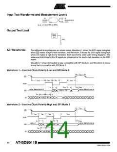
Input Test Waveforms and Measurement Levels
2.4V
AC
AC
2.0
DRIVING
LEVELS
MEASUREMENT
LEVEL
0.8
0.45V
tR, tF < 3 ns (10% to 90%)
Output Test Load
AC Waveforms
DEVICE
UNDER
TEST
30 pF
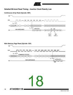
Two different timing diagrams are shown below. Waveform 1 shows the SCK signal being low
when CS makes a high-to-low transition, and Waveform 2 shows the SCK signal being high
when CS makes a high-to-low transition. Both waveforms show valid timing diagrams. The
setup and hold times for the SI signal are referenced to the low-to-high transition on the SCK
signal.
Waveform 1 shows timing that is also compatible with SPI Mode 0, and Waveform 2 shows
timing that is compatible with SPI Mode 3.
Waveform 1 – Inactive Clock Polarity Low and SPI Mode 0
tCS
CS
tCSS
tWH
tWL
tCSH
SCK
SO
SI
tV
tHO
tDIS
HIGH IMPEDANCE
tSU
HIGH IMPEDANCE
VALID OUT
tH
VALID IN
Waveform 2 – Inactive Clock Polarity High and SPI Mode 3
tCS
CS
tCSS
tWL
tWH
tCSH
SCK
SO
SI
tV
tHO
tDIS
HIGH Z
HIGH IMPEDANCE
VALID OUT
tH
tSU
VALID IN
14
AT45DB011B
1984H–DFLSH–10/04

 ATMEL [ ATMEL ]